


Why Citing Yield Without Die Area is Meaningless
Pat Gelsinger's field notes, and how defect density is a more meaningful metric for yield.


Right about a week after Pat Gelsinger left Intel late last year, he came back on X to comment on the right way to calculate yield, and was given a warm welcome by the internet being the highly technical and well respected industry titan that he is.

This led to a flurry of discussions online about the right way to calculate yield. Primarily, there seemed to be confusion when talking about yield in percentages which Gelsinger points out as a meaningless metric unless die size is also considered. A better way to talk about defects is in terms of defect densities (for which by the way, most foundries these days do not release actual numbers.)
In addition to all the recent news about the many possible futures of Intel, there has always been concern about yield on Intel’s 18A node, but the sentiment seems to be that the yield is good enough for big chips to be made on this node.
A few months ago, we discussed the different models used to calculate die yield.

In hindsight, we did not cover the importance of why defect density is the correct metric to use, and how area plays a role in die yield. This post attempts to fill in some gaps in understanding. We will cover:
Fundamentals
Yield depending on chip area
Calculating yields as defect densities
Example of yield calculations
Read time: 8 mins
This is a fully free post, but please consider upgrading to a paid tier to support the research and writing of articles such as these. Even one idea from this blog has the potential to pay for itself multiple times over!
Thanks to Jack Huang co-writing this post.
Jack Huang is currently an American Ph.D student who specialized in integrated photonics at UIUC. A Chicagoan by upbringing, education, and worldview, he holds degrees in physics and maths from UChicago. He is deeply passionate about American finance and technology with prior stints in quantitative trading and electro-photonic design automation (at Cadence). You can find him on Linkedin, Substack, or X.
Quick note: I am at the 2025 International Solid-State Circuits Conference (ISSCC) held in SF this week. Email me if you’d like to meet up. Always happy to chat!
Fundamentals
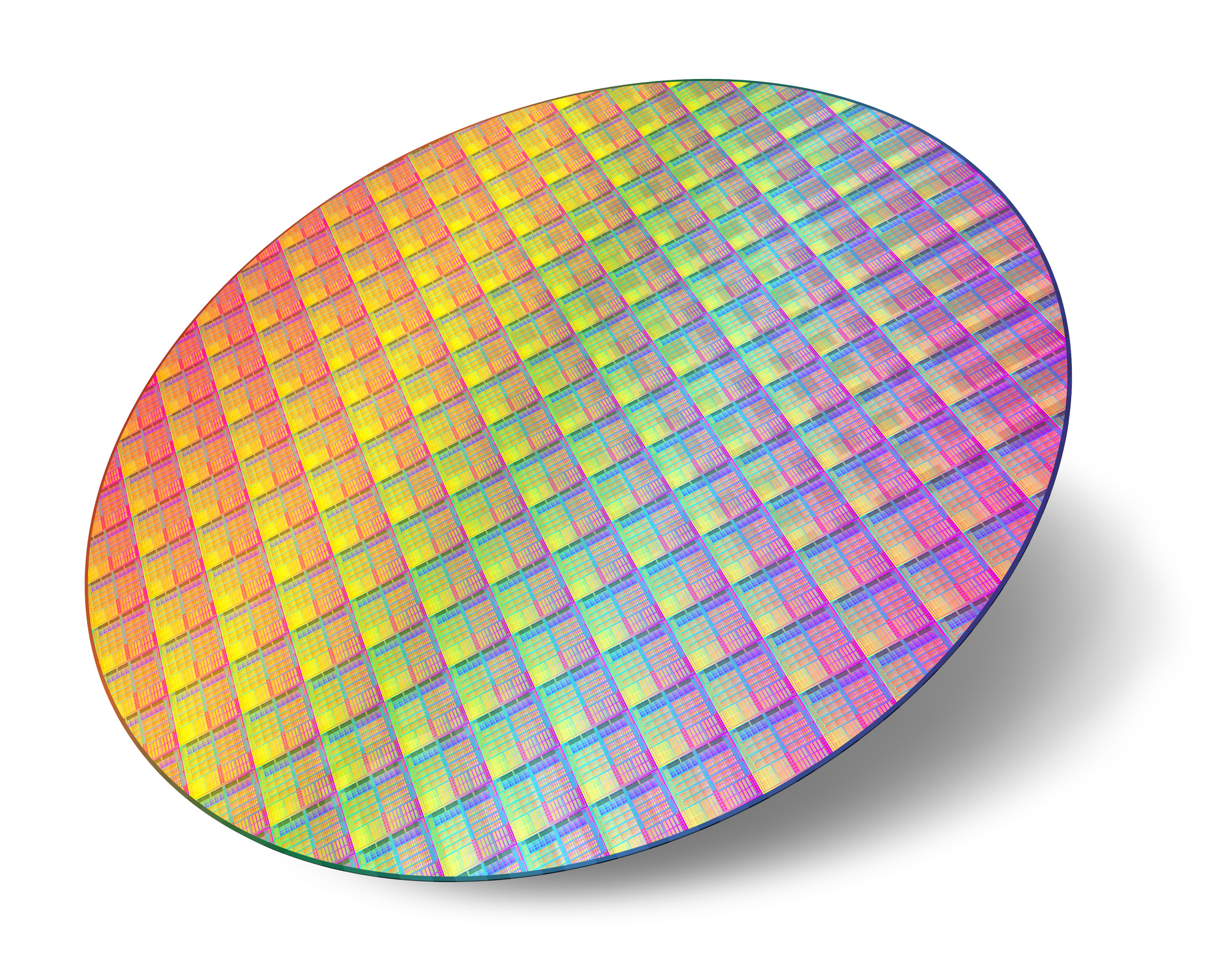
Chips are manufactured on thin discs of semiconducting material (for example silicon, gallium arsenide, silicon-on-insulator) called a wafer. These circular wafers are commonly 300 mm in diameter and have rectangular subsections called reticles with a maximum size of 858 mm2 (26 mm x 33 mm) for state-of-the-art technologies. You can simply think of a wafer as a circular pizza with rectangular cuts for each reticle. Any edge pieces or partial rectangles are useless and are discarded.
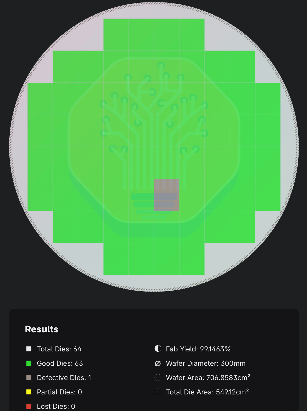
The size of each rectangle matters, and defines how large a chip can be. In applications such as GPUs, we want to put as many transistors on a chip as possible. In this case, a chip takes up the whole reticle and you get about 64 usable chips per wafer. There are plenty of applications where the chip size is smaller than the reticle. In such cases, a single wafer produces hundreds of identical chips. Interestingly, the Cerebras’ Wafer Scale Engine stitches together all the reticles on the wafer to produce one giant chip — but this is an unusual case.
Yield Dependence on Chip Area
Regardless of how big the chip is compared to a reticle, every manufactured chip needs to work as intended. If 10% of the manufactured chips fail to work or are sub-par in any sense, the yield is said to be 90%. From the pizza analogy, some rectangular pieces are just inedible. The reason that chips do not work as intended is because some part of the manufacturing process went astray, and the resulting defect causes the chip to fail.
But, companies do not always throw away subpar chips. They are often reclassified into lower tier product lines using a process called die yield harvesting or binning, but we won’t get into it here.
The yield when expressed as a percentage depends on the size of the chip we are talking about. Here is an example.
If the chip size covers almost the whole reticle (like in the case of a GPU) with a size of 858 mm2, one chip will fail while the other 63 are defect free. The yield in this case is 63/64 or 99.15%.
If the chip size were much smaller, say 225 mm2, then you get 256 fully formed chips per wafer, and a single defect on the wafer gives you 255/256 working chips or 99.77% yield. Notice how in this case you have partial die that are essentially non-functional.
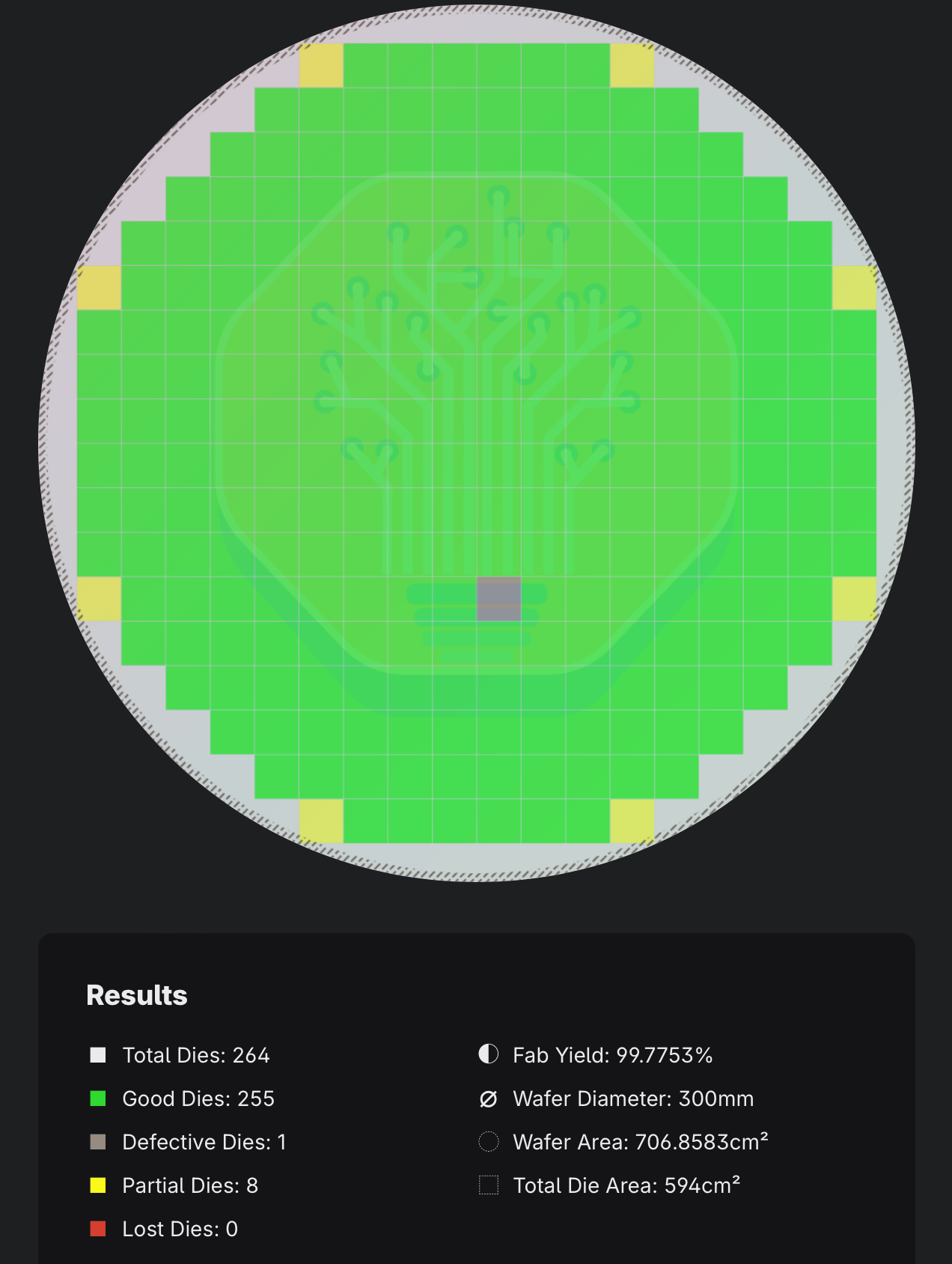


See how yield as a percentage looks better for smaller chips? In terms of accuracy of a wafer manufacturing process, they are exactly the same since they both produce only one defect per wafer. As the defect density increases, the yield numbers for large chips will look far worse than for smaller chips. Like Gelsinger said, yield as a percentage depends on the size of the chip.
The process of manufacturing a chip requires several hundred, highly controlled process steps – all of which need to go exactly as planned to have a fully functioning chip, often referred to as known good die. Only known good dies can actually be sold. So, the foundry needs to have sufficiently high yield in the process node before they can attract customers to make products on it.
If a wafer process takes 1000 steps, and each step has a 99.9% success rate, then the die yield is 0.999^1000 or 37%1. This gives a feel for how accurate the process steps involved in a wafer fab need to be. Each step in the process is highly optimized by experts in that particular process step (litho, etch, deposition) and is mostly tacit knowledge that is discussed little online or in public forums.
Hopefully it is clear that saying that a process’ yield is 90% is ambiguous unless you also specify the area of each chip. It is always better to talk about defect densities.
Calculating Yields as Defect Densities
One of the simplest models for defect density calculation is based on the Poisson distribution. The probability P that a chip on the wafer has ‘k’ defects is shown below. λ0 is the mean number of defects per die and for a fully working chip, there should be no defects. k! is the representation of a factorial in mathematics and is a concise way of saying k(k-1)(k-2)...1.
If you put k=0 in the above equation, P(0) is called die yield or DY. This quantity is actually measurable by a wafer fab which is simply the number of known good die per wafer. We can replace means defects per die λ0 with mean defects per unit area A called D0, so λ0=D0*A. D0 is called defect density and is represented as number of defects per square centimeter.
Putting this together, we get a relationship between a simple yield number DY and the defect density D0 which is most often referred to when talking about process yields.
Remember that DY is what you can actually measure in the fab, so to calculate defect density, we invert the equation as shown below.
From this equation alone, it is apparent that D0 is normalized to the area A of a chip and therefore represents a much more general figure-of-merit to how effective, profitable, and repeatable the process of wafer manufacturing is for any given process.
Example of Yield Calculations
The best way to understand how yield works is to play around with a yield calculator and put in some numbers. We used the same yield calculator for plots in the last section.
Here is an example set of parameters you can try:
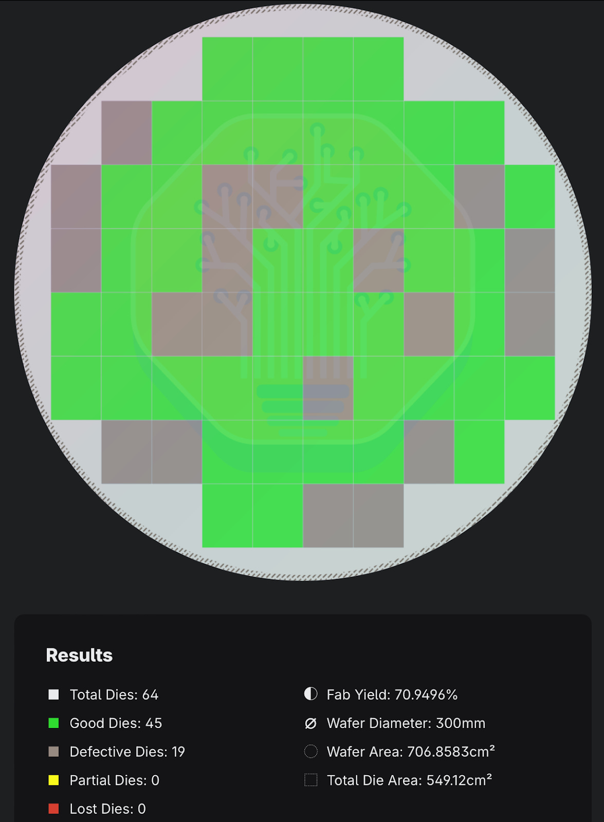
Die size: 26 mm x 33 mm (reticle limit; area = 858 mm2)
Wafer diameter: 300 mm
Defect density D0: 0.04/cm2
Yield model: Poisson’s model
This results in:
64 total dies
45 good dies/19 defective dies
~71% yield
You should try other numbers and yield models in the calculator to get an intuitive understanding for yourself. You can try to recreate the single defect cases from earlier.
At full reticle limit (chip area=858 mm2), a defect density of 0.04/cm2 gives you 71% yield. This is usually a pretty good number for a process node to be production ready. Foundries are generally secretive about their yield numbers and spend extraordinary amounts of effort to continuously improve it. This is for good reason too — yield directly impacts the bottom line of semi foundry business through the economic value high yields enable.
You can earn a 1 month paid subscription by recommending just two people to this publication using the button below.
We have a Discord community too! All free and paying subscribers are welcome.
The views, thoughts, and opinions expressed in this newsletter are solely mine; they do not reflect the views or positions of my past, present or future employers or any entities I am affiliated with. The content provided is for informational purposes only and does not constitute professional or investment advice.
This assumes that the steps are statistically independent from each other, which in reality, is not true. Still, the idea here it to point out how accurate the wafer processing steps need to be.
 | A guest post by
|
Thanks Vikram! A good reminder just how close to perfection a process has to be to avoid fabbing mostly expensive garbage. You already mentioned binning, which is crucial, especially for very large chips. The other factor is how sensitive or resistant the chip's design and function is to defects. A good design takes the likelihood of at least a few defects without losing function altogether into account. The other factor is the functional type of chip; for example, Nvidia's largest Blackwell GPU die is close to the size limit of the reticles TSMC currently uses for its EUV nodes, and probably the last monolith of its kind and size. A GPU die has, by its nature, many (thousands to hundreds) identical functional cores. Combine that with good design and great manufacturing, and the functional yield is still pretty good, despite having many billions of transistors per die. In contrast, a CPU (more functions, less redundancy) is a lot more sensitive to defects, as the likelihood that a fatal defect occurs in an essential and non-redundant function is much higher. Hence, the incentive of going to a chiplet/tile type design is greater for larger CPUs, despite the costs for the packaging required to get a functioning CPU.
As a request: a follow up article on how finished dies are tested and binned would be great - Thanks!
The ability to, for example, test individual chiplets is, of course, foundational for a chiplet design to actually make sense.