The Ultimate Guide to Accurate RFIC Simulations
A detailed analysis of what it takes to ensure that design simulations line up with reality, and achieve one pass design success.
Hey, I’m Vikram 👋 and thanks for reading! Reply to this email with your feedback. I love hearing from you. I also recommend joining other readers on Substack chat.
If you like these articles, please let others know. Word of mouth helps grow this newsletter! 🙏
In the previous post, we swiftly skimmed over the specifics of the actual design phase and overlooked one critical question.
How can we be confident that our simulations accurately reflect reality?
The solution consists in accurately modeling and validating the chip and its surroundings with simulation tools.
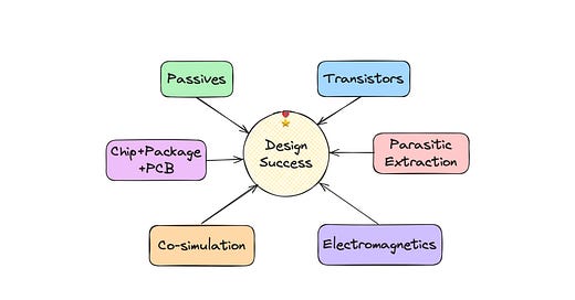
RF simulation and modeling are based on a few essential concepts, and when done correctly, can increase our confidence in design simulations.
Here is what we will discuss in depth:
Passive modeling of metal-dielectric structures using electromagnetic simulation
Active modeling of transistor devices using compact models
Combining the above using proper co-simulation strategies
Let's look at each one.
Passive Modeling
Anything passive refers to components that do not require electrical power to operate. They only attenuate signals, store energy, or provide a fixed impedance. Common examples of passive components include resistors, capacitors, inductors, and transformers. They are fundamental in filtering, impedance matching, and signal conditioning, and are largely made up of specific metal-dielectric combinations in three dimensions.
The behavior of these 3D structures to a radio frequency input is typically predicted using electromagnetic (EM) simulators. These tools are particularly capable of producing reliable predictions by numerically solving Maxwell's equations; however, the following must be accurately defined.
Metal and dielectric material properties: Information such as permittivity, loss tangent, resistivity, surface roughness, and permeability impact how electromagnetic fields interact with structures made of these materials.
Boundary conditions: Defines the state of the electromagnetic field at the simulation space's boundaries, as well as the suitable signal excitations along the simulated 3D structure.
Fortunately, the material properties of commonly used materials are well understood and available as a database in most EM simulators. The engineer has influence over the definition of boundary conditions, which should be carefully implemented.
Furthermore, all EM simulators provide a parameter that allows you to alter the degree to which the problem is discretized using a mesh. Finding the right extent for acceptable accuracy and reasonable simulation time is critical.
Before relying on the results of an EM simulator, engineers prefer to perform a one-time calibration operation. In this context, calibration entails ensuring that the material values, discretization settings, and boundary conditions used accurately predict hardware measurements in the laboratory.
The specific verification process varies based on the RF product being designed and the calibration of the EM simulator. Here are some popular approaches for RFICs:
Transmission lines: Coplanar waveguides are simple to measure with RF probes and construct on-wafer. Determine the RLGC parameters from the measured s-parameters and compare them to those obtained from simulations.
Inductors: Spiral inductors of various sizes and shapes are useful for verifying the simulation's material parameters. The main goal is to align the self-resonance frequency, quality factor, and simulated inductance with the measurement.
Capacitors: Dielectric constants on wafer can be extracted by simulating metal-oxide-metal (MOM) or metal-insulator-metal (MIM) capacitors (plate or interdigitated). The simulated capacitance and Q-factor should match measurement.
Resonators: Resonators are helpful since they combine inductors and capacitors. Usually, the resonant frequency is adjusted to a point where routing parasitics become significant. When EM simulations accurately determine the resonance frequency, all parasitic elements are included, and the simulation can be considered reliable.
Any EM simulator's accuracy can be confirmed with sufficient rigor to a high degree of certainty. Complexity arises when amplifying devices are used.
Active Modeling
The electrical model of an amplifying device such as a MOSFET or bipolar transistor is far more complicated than the small signal models often shown in textbooks. The simple model does not account for all the physics of a transistor, will not scale properly with device sizing or support advanced nonlinear simulations.
In practice, device models consist of extensive equations implemented in Verilog-A or C. The equations are based on the analytical equations for currents and charge storage, and are designed to mimic the behavior of an actual transistor. As much as we would like these models to be physics-based, charge transport in modern devices is so complicated that non-physical fitting factors are often required.
These “compact models” are normally provided by the foundry, which hires a team of device modeling experts to extract them. The function of the device modeling engineer is to determine the coefficients of the equations so that the model can predict the current and charge dependence on voltage, temperature, and frequency. Fitting device models typically necessitates comprehensive device level measurements.
The BSIM model family is the industry standard for MOSFETs, with several hundred parameters that must be selected to accurately forecast various operating zones and effects in a transistor. The HiCUM model for BJTs contains more than 130 parameters.
How are these models validated?
Device models are frequently either unvalidated or only partially validated. Design teams place implicit trust in them because it takes many transistor-level measurements to validate that the model is sufficiently precise. Some businesses may have the funds to support a small team of device modeling professionals who will place transistors on test vehicles, measure them, and validate them against the foundry model. They will also make internal adjustments to the model as needed.
In my opinion, the best method to assess a model's accuracy is to develop reference designs, such as an amplifier on a test vehicle, and then see if the model predicts the DC, s-parameter, and nonlinear performance of the reference amplifier. The reference amplifier can be configured for low-current mobile applications, high-current infrastructure applications, or anything in between.
I've done a lot of this, and the accuracy with which device models predict these "real" circuits is often crucial to an RFIC designer. This exercise quantitatively exposes problems in a device model, particularly nonlinearity, which is difficult to detect using only device-level data.
The essential point here is that you should never blindly trust what device model simulations tell you. Foundry models are typically pretty good, however this varies depending on the foundry, the technology node, and the level of precision required. Comprehensive validation of device models is required before they are deployed in multi-million dollar projects.
Co-simulation
Another advantage of using a reference amplifier design for device model validation is the ability to validate active and passive modeling at the same time. Inductors, transmission lines, and capacitors are common components of amplifiers, and the process of connecting an active device to a passive model is known as co-simulation.
Co-simulation is necessary because electromagnetic simulators cannot handle transistor-level physics. Active and passive models must be blended in a circuit simulator to capture the unwanted circuit interactions (or parasitics) needed to accurately predict circuit performance. Keysight has a bunch of video lessons on EM-circuit co-simulation if you want to go deeper.
In general, parasitics need to be captured at three levels: transistor, circuit and board/PCB.
1: Transistor Level
The transistor model for any active device is made up of two parts:
Intrinsic: This describes the device's basic behavior. This is precisely what we described in the active modeling section, where equations govern how the device responds during simulation. It may also include some parasitic capacitances up to a pre-defined metal level.
Extrinsic: This section of the model defines all of the parasitic elements associated with the transistor that are not related to the device's core function. This often includes capacitances between metal connections not included in the intrinsic model.
In practical chip layout, it is necessary to use other metal levels to make connections on the chip. The associated parasitics need to be included in simulation. An EM simulator is a possible solution, but the complexity and narrow feature sizes involved in transistors make it a resource intensive task. Also, the high simulation overhead of EM simulators may be overkill for device parasitics extraction.
Instead, industry-standard EDA programs include a parasitic extraction tool that can be used to obtain extrinsic parasitics. These parasitic extraction tools aren't field solvers. They employ a pattern matching technique to extract capacitance from a pre-trained dataset. It is critical to identify where the device model ends and the parasitic model begins in order to avoid under or overcounting parasitic elements.
The table below shows capacitances in a FinFET that are either included in the compact model or extracted via parasitic extraction.

2: Circuit Level
This phase in parasitic modeling is critically necessary. Whether you're building an RF circuit off-chip or on-chip, you must account for every connection and passive component in the context of everything else.
Here is a list of frequently encountered problems that need careful attention.
Inductors have massive electromagnetic fields and can couple to various portions on the chip.
Metal seal rings used to enclose chip designs can provide a coupling path to various unrelated parts of the chip.
Large bypass capacitors when placed next to inductors appear as ground planes and can alter their inductance value.
If density fill cannot be avoided, the additional capacitance must somehow be accounted for.
The major challenge is connecting active devices to the circuit-level EM model. The manner in which you establish ports for transistor terminals has a significant impact on simulation accuracy. Ports cannot always be "calibrated out" and frequently have an impact on the circuit. The purpose of co-simulation is to reduce the impact by creating the shortest possible return path for current by selecting appropriate ports. You should also verify that the EM model contains enough low frequency data to ensure the circuit's DC convergence.
When you co-simulate your design, you may notice a drop in performance on several critical metrics. Interactions between passive elements provide undesirable signal pathways, which must be identified and eliminated via iterative EM co-simulation. The more you focus on EM co-simulation, the better your chances of design success.
3: Package / Board Level
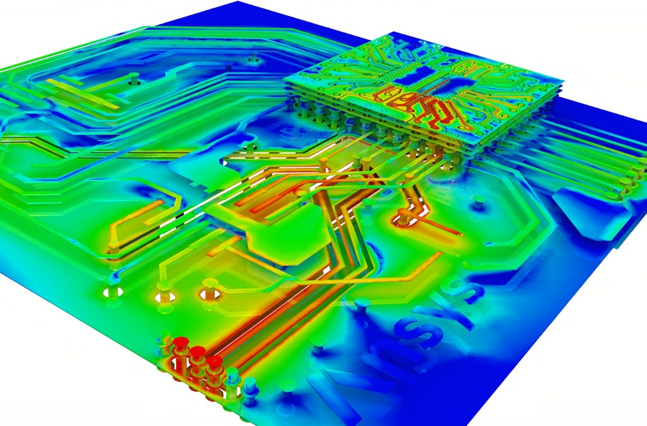
The chip will eventually need to be packaged or integrated into a final module. This is ultimately what will be used to measure chip performance or determine whether the chip meets the requirements of the module it is in. The impact of the package or module on chip performance must be considered using EM simulation.
In wirebond packaging, there are wires of metal that connect the chip to the package which can interact with each other. In flipchip packaging, the chip is flipped upside down and attached with solderballs to a package or module. Doing so often brings the ground plane of the package much closer to the on-chip metal lines and impacts the its electromagnetic field.
Chip-package EM co-simulation becomes critical for capturing such interactions. This is significantly more computationally intensive since you must integrate narrow dimension traces on-chip alongside the enormous feature sizes of a package in the same simulation.

Finally, when the chip is put on an evaluation circuit board with connectors, it is recommended to simulate the entire board in an electromagnetic simulator. You will need to account for connection to trace transitions, and trace to package transitions. Simulating a chip, packaging, and whole board simultaneously is difficult due to the relative scale of dimensions involved. At the very least, the board should be simulated by itself to ensure that it is sufficiently well constructed to allow correct chip measurement during testing.
The Wrap Up
There are a few other factors to consider that we have not addressed here. Depending on your RF circuit, you will most likely need to include heat and mechanical impacts in your design. Electrothermal analysis plays a critical role in power amplifier simulations. Mechanical design of heat sinks and heat flow analysis could also be relevant dependent on your power dissipation requirements. There are a variety of tools that support multi-physics simulations depending on the design needs.
Even if you completely follow the guidelines in this article, your simulations may not exactly match the observations. In that case, take the time to figure out why. Incorporate the insights into your next design cycle.
This iterative technique makes RF design both tough and rewarding.
🔑 Key Takeaways
Accurate modeling of passive and active components using electromagnetic simulators and detailed device models is essential for RF simulations.
Rigorous validation against real-world measurements ensures the reliability of both passive and active simulation results.
Co-simulation is crucial for capturing interactions between active and passive elements, addressing parasitics at transistor, circuit and package levels for accurate circuit performance predictions.
RF engineering is an iterative process where you include learnings from each design cycle to improve the next.
The views, thoughts, and opinions expressed in this newsletter are solely mine; they do not reflect the views or positions of my employer or any entities I am affiliated with. The content provided is for informational purposes only and does not constitute professional or investment advice.


