


How Electrons Move in Semiconductors: The Science of Carrier Drift
Understanding the forces, scattering mechanisms, and mobility factors that govern charge transport.

This article is part of The Joy of Semiconductor Devices series — a collection of posts that explains the inner workings of semiconductor technology from first principles in an accessible manner.
Table of Contents:
Mechanism of Carrier Drift
Charge Mobility
🔒 Scattering and Dependence of Mobility on Temperature
Lattice scattering
Impurity scattering
Total mobility (lattice + impurity)
🔒 Further reading
Read time: 4 mins (free), 8 mins (paid)
Here is the previous post in the series.

Mechanism of Carrier Drift
In the last post, we looked at a piece of intrinsic or extrinsic (with doping) semiconductor in equilibrium, which means that there is no external stimulus applied. In such a material, electrons and holes are randomly moving within the crystal structure, colliding with atoms and doping impurities. In this post, we will assign two numbers to quantify these collisions:
Mean free path: This is the average distance travelled by a charged particle before it undergoes collision with an atom or impurity.
Mean free time: This is the average time a charged particle travels before it undergoes a collision.
The moment we connect the terminals of the semiconductor to a battery, many interesting things start to happen. Understanding each one will lead us to an understanding of carrier mobility — a fundamental concept in semiconductor physics — and its dependance on temperature and doping level.
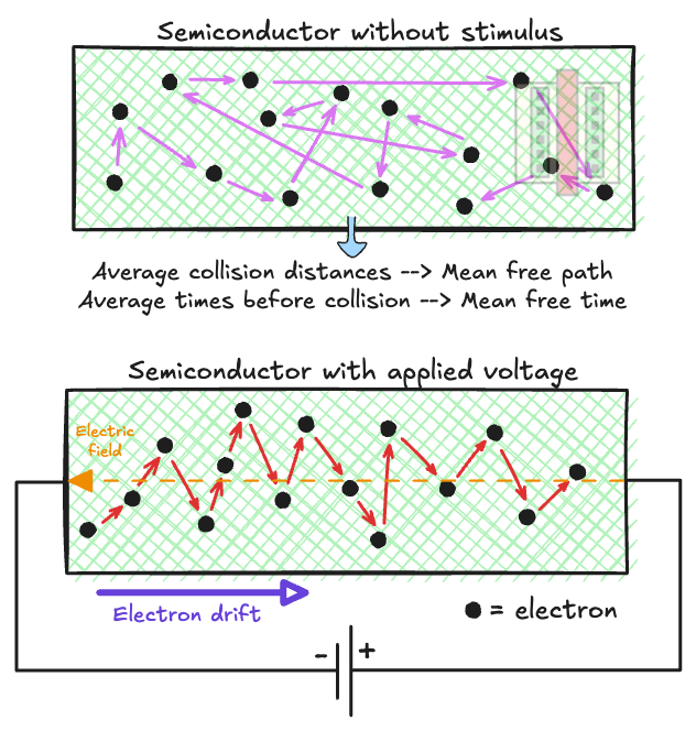
The voltage across the battery terminals induces an electric field (E-field) that goes from the positive to the negative terminal of the battery. The randomly moving charged particles, still colliding with each other, now start collectively moving towards the battery terminals; electrons get attracted to the positive battery terminal, and holes to the negative battery terminal. In other words, electrons drift against the direction of the E-field, and holes drift along the direction of the E-field.
Notice the use of the word drift. The E-field applied in the semiconductor does not cause charged particles to rapidly accelerate towards the battery terminals because of continuous scattering with the atoms of the crystal lattice. The net effect is that there is a collective movement of charge, while still undergoing random collisions along the way, towards the terminals of the E-field applied.
This carrier transport mechanism is called drift, and the speed of the collective movement of charge is called drift velocity. To give a physical sense of how fast carriers collectively move: drift velocity is 2-3 orders of magnitude slower than the velocity of electrons undergoing collisions within the material due to thermal agitation.
Charge Mobility
Now that we understand drift, let's define how easily charge carriers move within a semiconductor—this is called mobility, and is arguably one of the most important quantities in all of semiconductor physics. The current generated by a transistor in response to input voltage is directly proportional to mobility, and a higher current (mobility) has important implications:
In digital design, higher mobility allows for faster switching and higher clock speeds. This often allows the use of lower supply voltages reducing power dissipation.
In analog design, higher mobility allows amplifiers to have higher gain, operate at higher frequencies and have lower distortion.
We saw that applying an external field makes charges drift. From a microscopic view, when an electric field of strength E is applied to an electron with charge -q (charge of an electron is negative), it faces a force -qE. If this force is applied for a time period between collisions (called mean free time, tc) the electron gains a momentum -qE times tc.
If the electron has an effective mass mn, and a drift velocity vn, these quantities can be equated as
or, we can get an expression for drift velocity as,
This is the expression for drift velocity. To be clear, the effective mass (mn) of a charged particle is the mass of the particle under the influence of the crystal lattice, which is different from free mass of a charged particle in vacuum. The effective mass also differs depending on the semiconductor material.
Let us make some observations to understand drift velocity intuitively:
More E-field, more drift velocity
If a higher voltage battery is connected, or the piece of semiconductor is made thinner, the higher E-field imparts a stronger force on the electron, causing it to move faster.
More mean free time, more drift velocity
If the charged particles can move around without constantly colliding with the lattice, then it makes sense they can move faster in response to the applied field.
Lower effective mass, more drift velocity
If the charged particle is lighter, then it moves faster.
More importantly, the proportionality factor that relates drift velocity to E-field is called electron mobility and is given by:
What are the units of mobility? Remember that mobility is the ratio of drift velocity (m/s) to electric field (V/m). This makes the units of mobility m2/V-s, although it is more commonly expressed in the units of cm2/V-s.
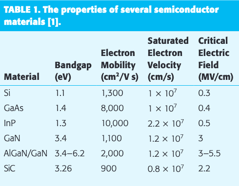
For example, the mobility of silicon at room temperature is approximately 1,400 cm2/V-s. The same principles apply for holes, except that the negative sign is removed and holes travel along the direction of E-field while electrons travel against. The mobility of holes is lower than electrons (~450 cm2/V-s) because the effective mass of holes is higher than electrons.
Mobility is not a fixed number and varies strongly with semiconductor material, temperature and impurity doping concentration.
Scattering and Dependence of Mobility on Temperature
We have been rather vague so far about how the lattice of atoms affects the movement of electrons (or holes) through it. When a charged particle moves through a lattice, it is subject to two kinds of scattering, both of which impact mobility differently across temperature.