


NVIDIA CuLitho and the Future of Inverse Lithography
How GPU-scale compute is reshaping mask synthesis for advanced nodes.

NVIDIA announced CuLitho in the 2023 GTC conference. With its seemingly silly name (not an April fool’s joke), CuLitho is a GPU-acceleration software library used to speed up the process of making the masks used for chip manufacturing. At the 2024 GTC, there was news again that CuLitho accelerates compute-intensive foundry operations by 60x with Dr. C. C. Wei, CEO of TSMC announcing,
We are moving NVIDIA cuLitho into production at TSMC, leveraging this computational lithography technology to drive a critical component of semiconductor scaling.
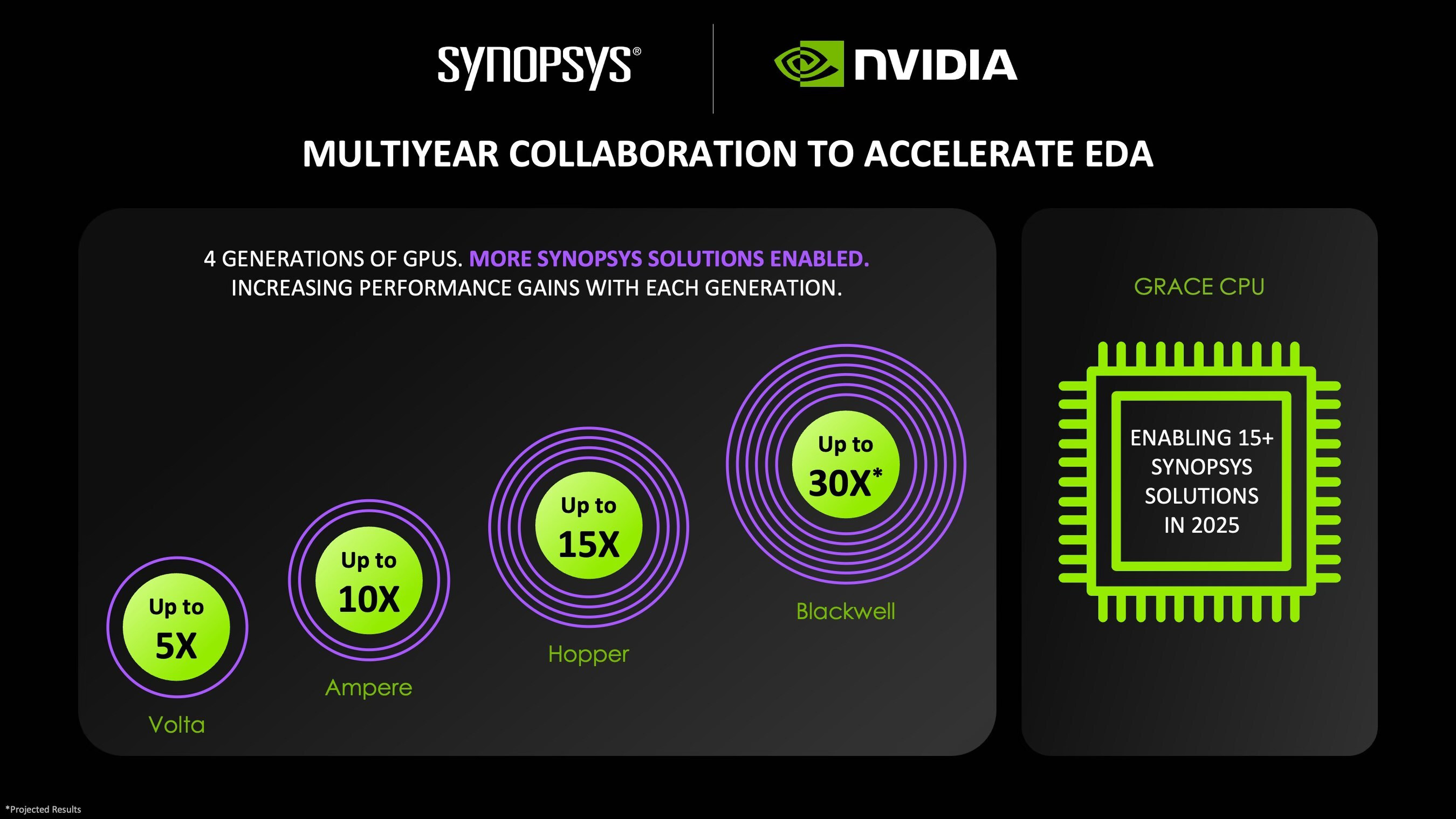
Recently, Synopsys announced that they are using the Blackwell series GB200 chips across a number of their workflows in device and circuit simulation, and computational lithography. While CuLitho kept popping up in the news, my rudimentary background in semiconductor manufacturing did not allow me to truly appreciate this development. So I looked into it.
I went down the computational lithography rabbit hole for a couple of days and realized I should have started with the excellent video below by Asianometry explaining the use of NVIDIA chips for lithography. I almost didn’t write this post since the video was so good but ended up doing it anyway because of good folks online who encouraged me to explain it my way, and add to it if possible. So I did.
This post is my understanding of how inverse computational lithography works, and the role of GPU-acceleration in the future of semiconductor manufacturing.
Here is what we will discuss:
Lithography, critical dimension and Rayleigh criterion
Optical Corrections in lithography
Inverse lithography technique (ILT)
🔒 GPU acceleration and the future of ILT
Read time: 11 minutes
Lithography, Critical Dimension and Rayleigh Criterion
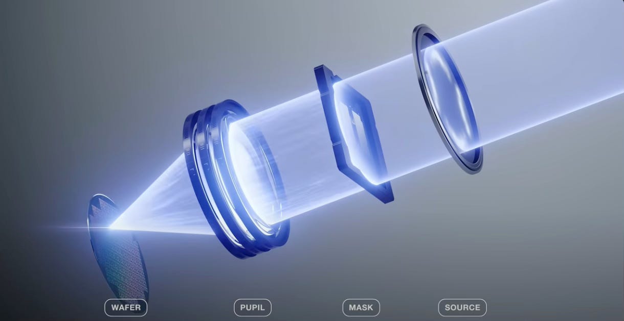
Lithography is the process of patterning tiny geometries on a silicon wafer that enables us to create modern day transistors with nanometer scale feature sizes. Much like a photo was processed in the early days, the process of lithography needs a mask, which is like a film negative.
The purpose of the mask is to allow light to pass through in some areas, while blocking it in others. Features are formed on the wafer depending on its interaction with the light. Thus, to pattern intricate electronic circuits we need many masks corresponding to the geometries required on various levels on the silicon wafer. For example, a TSMC 5nm process with EUV requires 81 masks with an approximate cost of $100K+ per mask.
To fully understand the process of chip manufacturing, I recommend that you check out the following YouTube video that has some fantastic animations.
Ideally, we would like to make geometries on a silicon wafer as small as possible so that we can cram a lot of them into a small area. But the smallest feature size we can make using a lithography system is called the critical dimension or CD, which is governed by the Rayleigh criterion.
We want to make CD as small as possible and to do this, we have a few knobs to turn.
Wavelength (lambda): This is the wavelength of light used for the lithography process. For example, using 193 nm Argon Fluoride excimer lasers in combination with immersion lithography was a major step towards the miniaturization of transistors. Today, extreme UV (EUV) lithography uses 13.5 nm light generated by blasting tin droplets with laser light.
Numerical aperture (NA): This is a measure of the total range of angles over which a lens can collect light. A high NA lens increases the resolution of the features that can be patterned, but has reduced depth of focus. A very shallow depth of focus means that even small thickness changes in wafer thickness will affect lithography which is undesirable.
k1-factor: This is an factor that represents all the other techniques used in a lithography process to improve resolution. From an optics perspective, physics limits the lower limit of k1 to 0.25, although there are ways to get around this limit using lithography techniques.
k1 factor is what semiconductor foundries try to improve using tricks in the lithography steps so that smaller features can be accurately manufactured on a wafer. We will discuss some of these tricks next.
Optical Corrections in Lithography
Unlike a film photo, the negative mask looks quite different from the patterned features in a leading edge lithography process. The reason is that light at the nanometer scale diffracts, and without corrections to the mask, the patterned geometries would be a blotched mess. The 'pre-correction' to the mask is done using a process called Optical Proximity Correction, or OPC. The picture below shows how the mask shapes required to print a simple cross pattern have evolved. Let’s talk about each evolution some more.
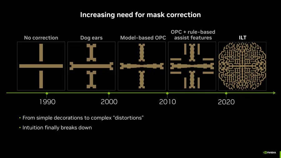
#1: Rule-Based
Rule-based OPC relies on a predefined set of rules to modify the mask layout. These rules are formulated via trial-and-error by comparing the mask layout to the patterned shapes, and making adjustments to the mask till the correct patterned shapes are printed. The example below shows a simple dog-ear modification to the mask. This method worked well till around the 130 nm node, and started to breakdown at the 90 nm node.
#2: Model-based
As transistor gate length scaled down to about 65 nm, model-based OPC correction became the de-facto standard. This correction method was devised based on extensive simulation-based compact models that could predict the patterned shapes based on the mask layout. It could make more complex corrections to the mask to enhance the resolution of patterned shapes. Eventually, the heuristics from rule-based approaches was included along with model based approaches as transistor nodes scaled to 45 nm and below. The need for computation to create masks led to the rise of computational lithography techniques.
#3: Sub-Resolution Assist Features (SRAFs)
SRAFs are features on a mask that don't actually result in printed features because they are sized below the resolution limit of the lithographic system. Their main purpose is to influence the diffraction patterns of light during exposure to improve the resolution and accuracy of printed patterns.
SRAFs can be used with rule-based, model-based or ILT approaches and are a key component of OPC. The placement of SRAFs on a mask is determined by lithographic simulations and can be quite compute intensive.
Now that we’ve seen how traditional mask corrections evolved, let’s look at the next frontier — inverse design.
Inverse Lithography Technique (ILT)
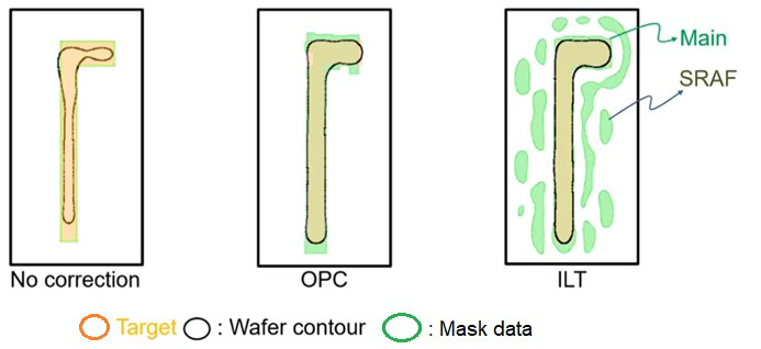
As transistors further scaled down, inverse lithography techniques (ILT) became essential. To produce any pattern on silicon, the mask design looked entirely different from the intended geometry and was completely unrelated to what intuition would have you believe. Instead of starting with a mask that looks like the shape being patterned and then trying to make adjustments to it, ILT reverses the process instead asking the question:
What is the optimal shape of optical mask that results in the closest intended shapes in silicon?
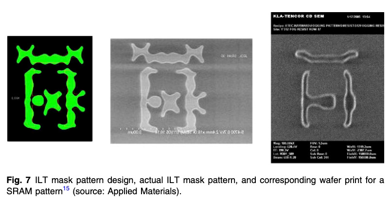
The important aspect here is that there is no constraint that the mask should even remotely resemble the final feature shape, and many unique mask shapes may result in the same final features1. The image below shows how an ILT design mask pattern looks, and how the final pattern forms on silicon based on this mask. You can see there is no intuitive link between the two, other than the overall general shape if you squint.
The concept of ILT has been around since the 1980s but the first commercialization of ILT into semiconductor manufacturing was by Luminescent Technologies in 2003. By 2010, three companies were dominant in ILT: Luminescent, which was bought by Synopsys in 2012, Intel who called it the "pixelated mask method", and Gauda, which was later acquired by D2S Inc.
ILT was revolutionary when it was introduced, but it was not adopted immediately for a couple of technical reasons.
Finding the right shapes on the ILT mask needed a massive amount of compute
Higher complexity meant that writing the mask took a huge amount of time
Most importantly, the arrival of 193 nm Argon Fluoride (ArF) immersion lithography meant that smaller features could be patterned without the need for complex ILT masks. As a result, ILT was mostly used for niche applications like memory cell-array printing, in logic for 'hot-spot' repair, or as a golden standard to improve traditional OPC.
As technology nodes evolved to 7 nm and below, the small resolution required the increasing use of ILT designed masks. The computation needs are extremely challenging given that a chip has millions of patterned features on it, and a mask to create it has to be inverse designed. Even if a process like TSMC 5nm has 81 masks, ILT is only used for a few critical masks due to its complexity.
The use of ILT requires foundries to have their own data centers with tens of thousands of CPUs working for tens of billions of hours every year to determine the right mask patterns required to manufacture at leading edge logic nodes. The need for compute in lithography is still on the rise, but luckily the advent of GPU acceleration has opened up a world of possibility.
GPU Acceleration and the Future of ILT
The amount of image processing and compute required for ILT makes GPU acceleration a perfect candidate to improve the efficiency of computation. We will explore what the benefits of GPU acceleration are for the future of lithography, identify some key companies, and provide additional research resources after the paywall.