How Tuning, Filtering and Switching helps your Smartphone deal with 50+ Unique Frequencies
The received signal from the antenna can take 100+ different paths through the RF front end. Tuners, filters and switches make the magic happen. Learn how.
Hey, I’m Vikram 👋 and thanks for reading!
Reply to this email and let me know about questions you have, topics you’d like to see or challenges you are facing. The feedback will help me improve the content quality. Even a few sentences will do! I reply to every email. 📝
You can also reach me on LinkedIn/X or join the community on the Substack chat.
If you like these articles, please let others know. Word of mouth helps grow this newsletter! 🙏
It is incredible how many standards your smartphone has to support.
Communication standards are many. GSM, CDMA, LTE, GPS, WiFi, 5G, Bluetooth, mmWave. And then you have frequency allocations by provider and geographic restrictions. Often they have to work simultaneously, like when you need to listen to music via bluetooth and have GPS navigation at the same time.
The secret to all of this is proper signal selection in the radio front-end, which constitutes the electronics right after the antenna in the superheterodyne system.
In this post, you will learn the basics of:
Antennas and Tuning
Front-end Filtering
RF Switching
Antennas and Tuning
A modern smartphone operates over 50 bands ranging from 500 MHz to 6 GHz and utilizes 6 to 8 antennas to cover the wide range of frequencies involved. Innovative antenna designs are required and in addition, the antenna needs to be tuned to increase its efficiency, radiated power and range.
Antenna tuning involves the use of a bank of capacitors (sometimes inductors too) with semiconductor switches that can be turned on or off with digital control. Depending on the requirements, the capacitors are either discrete components or integrated on-chip with the switch. The digitally tunable capacitor bank is placed at various points in the antenna to optimize its performance.
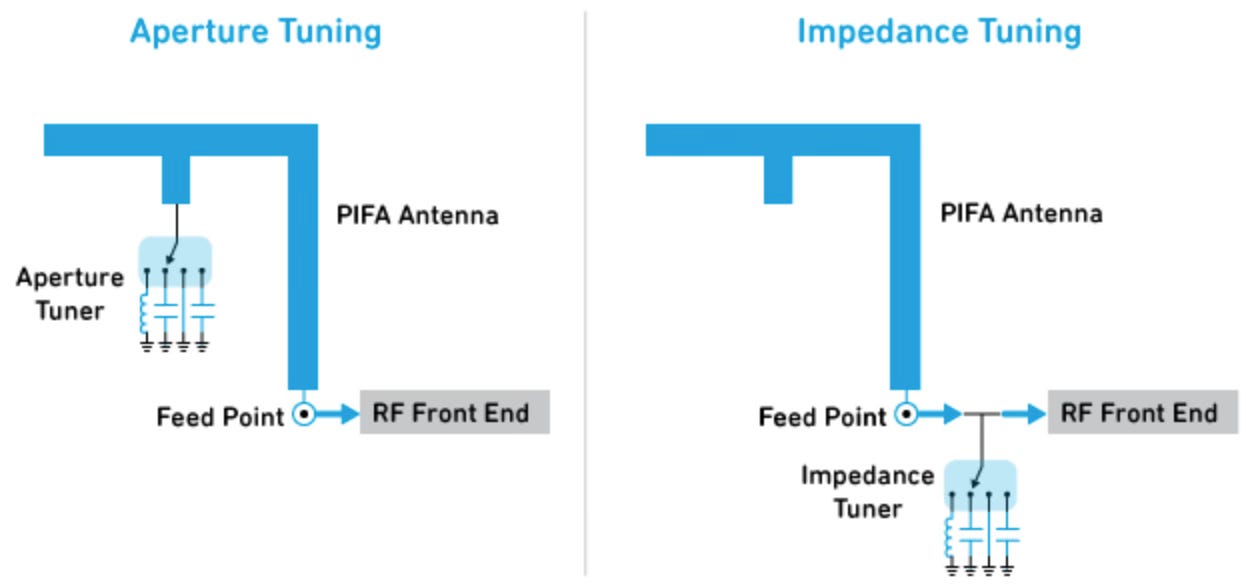
Tuning the bank of capacitors enables two functions in the antenna:
Aperture tuning: The natural resonance of the antenna is shifted to the required band of operation thereby increasing its overall efficiency. If required, the antenna can be made to operate over two bands simultaneously for carrier aggregation.
Impedance tuning: Optimizes the signal transmission to the antenna by providing the correct impedance environment between the antenna and the rest of the system. It even compensates for the way the phone is held by the user, so that antenna performance is not affected (remember antenna gate?).
Antenna tuners need to be low loss since they are directly connected to the antenna, and can drastically impact signal to noise ratio in the receive path, or overall system efficiency in the transmit path.
The RF switches also need to have low capacitance so that the capacitance tuning range is only set by the discrete capacitors being switched. Otherwise, the tuning range (represented by C-max/C-min) becomes limited, and the antenna’s tuning range is also reduced.
Since the antenna tuners appear after the power amplifier in the signal chain, they need to be able to handle high power while producing minimum distortion through nonlinearities.
A lot of such antenna tuner switches are implemented with Silicon-on-Insulator (SOI) technology become of the low-loss and low-capacitance switches that can be implemented on it. We will revisit the switch implementation later in the article.
Front End Filtering
A modern 5G smartphone has over 300 total RF paths and utilizes over 25 filters to reject unwanted frequencies from the received antenna signal. Within each GHz frequency band in a communication standard, there are channels with bandwidths of 10-100 MHz containing information that needs to be extracted.
Ideally, we would like to filter out only the specific channel from the received signal. However, this would require a filter with exceptional rejection, which in most cases is not even achievable. Even if it were, higher rejection levels in a filter can only come from increasing the filter order, which increases filter loss.
This is an unacceptable system penalty to pay especially for components that come between the antenna and amplifiers. The generally accepted solution is to just filter the entire frequency band and not a specific channel, in order to remove unwanted interference. The bandwidth of the filter relative to its center frequency will be 5-10% which is much more reasonable to implement in practice.
Interference can be of two kinds:
Out-of-band interference: These are unwanted signals present in the radio spectrum that do not belong to the communication standard of interest. For example: A GPS signal around 1.5 GHz would be out of band interference to a WiFi signal at 2.4 GHz.
In-band interference: These are unwanted signals present within the frequency band of interest and usually present due to communication signals in neighboring closely spaced channels.
Only out-of-band interference can be easily rejected by filtering in the front-end. If the in-band interference is sufficiently far away in frequency, it may be filtered in the front-end. Otherwise, it will be handled elsewhere in the RF receiver system.
Filtering in the front-end of the radio system is usually implemented with acoustic wave filters. They work by converting an electrical signal to an acoustic signal, which then travels across the filter, and is converted into an electrical signal again. These filters are several orders of magnitude smaller than electromagnetic wave filters and are ideal candidates for portable communication devices. They have low loss and exceptional rejection.
They are of two types:
Surface Acoustic Wave (SAW) filters: Cheaper to implement and less complex but limited to about 2.5 GHz in center frequency.
Bulk Acoustic Wave (BAW) filters: More complex 3D structure and costlier but can be implemented to even 10 GHz and beyond. They offer better performance than SAW filters for applications below 2.5 GHz.
The figure below shows the interdigitated metal fingers used on a piezoelectric substrate to design a SAW filter. The response of a typical BAW filter for WiFi operation shows that over 40 dB of rejection can be achieved for neighboring frequency bands.
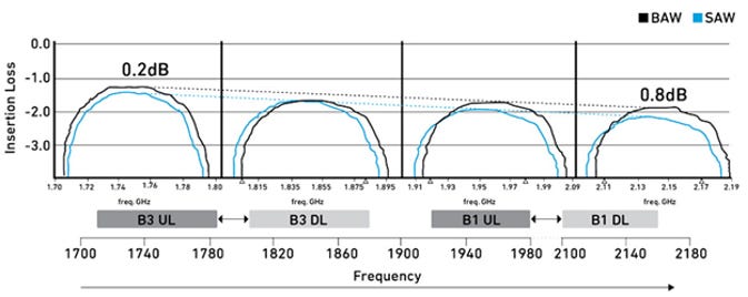
The figure below shows a comparison of insertion loss between SAW and BAW filters. The typical loss of these filters is 1-2 dB, and loss improvements of even tenths of a dB are significant for such filters. These filters are used extensively in the RF front-end system to isolate various frequencies of operation and allow coexistence between the various communication standards.

RF Switches
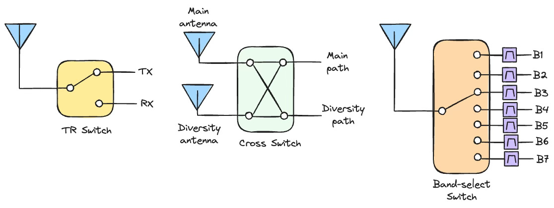
There are various kinds of RF switches used in a practical RF front end that perform different signal switching functions. Some of them are:
TR switch: These switches are used in a time-domain-duplexed (TDD) system to switch between transmit and receive paths, where only one of them operate at any given instant.
Antenna diversity or cross switch: These switches are used to connect different antennas to the receiver circuits depending on which antenna is providing superior performance at any point in time.
Band select switch: These are switches that connect the received signal to various SAW/BAW filters appropriate for the band of operation.
Depending on how many switching paths it provides, switches are defined by “Poles” and “Throws.” I like to think of it this way:
Poles: how many paths you are switching from.
Throws: how many paths you are switching to.
In the above example, the TR switch would be single pole dual throw or SPDT. The cross switch would be dual pole, dual throw (DPDT). The band select switch would be single pole seven throw (SP7T).
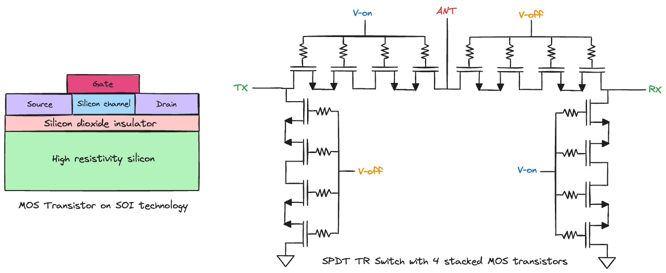
These switches are similar in construction to the antenna tuners we looked at earlier. MOS transistors on Silicon-on-Insulator (SOI) technology are a popular choice for the implementation of these switches due to the low loss and high isolation they provide.
Unlike conventional bulk silicon used for digital electronics, SOI technology uses a thin layer of silicon dioxide between the transistors and the silicon substrate they are built on. Silicon dioxide itself is a poor semiconductor, and thus “insulates” the transistor from the detrimental effects of the substrate.
Internally, each switch consists of a bunch of MOS transistors connected in series as shown in the figure above. A high valued resistor is used at the gate of each transistor to insulate the gates from each other. Transistor stacks in shunt are used to sink any leakage of RF signals through the off transistor stacks in series, and improve overall isolation.
Each transistor has an on-resistance (R-on) and off-capacitance (C-off) that is strongly determined by the construction of the transistor. The product of R-on and C-off is a key metric that foundries try to minimize in a transistor. Also, each transistor is capable of withstanding a specified voltage before it breaks down.
The power handling capability of the switch is determined by how many transistors are stacked in series. If it needs to withstand a peak RF voltage of 10V and each transistor can handle 2.5V before breakdown, you will need 4 switches in series. By stacking more transistors, you increase the overall R-on of the switch 4-fold, and its insertion loss is higher.
Higher number of poles and throws in a switch increases the overall capacitance of the switch. For example, in an SP7T, the pole end of the switch would see the off-capacitances of all the six other throws when connected to a single throw.
Lastly, since these switches use MOS transistors, there is an inherent nonlinearity associated with them which results in harmonic frequency generation. A lot of research has gone into minimizing these harmonics with design techniques and use of highly linear materials in the construction of the transistors (see one reference below).
In summary, the design of a switch is an intricate process carefully balancing the loss, isolation, linearity and power handling specifications to meet the requirements of the application.
🔑 Key Takeaways
The RF front end in a communication system performs tuning, filtering and switching functions to maximize signal to noise ratio and minimize distortions.
Antenna tuners maximize efficiency by dynamically tuning antenna aperture or impedance. This also helps in effective antenna reuse between different bands.
SAW and BAW filters are the workhorse for filtering functions in mobile communications due to their low loss, high selectivity and small size.
RF switches ensure that the appropriate connections are made from the antenna to the amplifier systems in the radio with minimal loss and distortion.
📚 References
RF Front End Module Architectures for 5G - Skyworks paper on RF front end architectures for 5G smartphones
RF Front End Components and Limitations - Explains key parameters, design and tradeoffs of front end components.
Wireless Communication Application Guide - This white paper from Infineon has some great block diagrams to understand the RF front end.
A SPDT RF Switch Small- and Large-Signal Characteristics on TR-HR SOI Substrates, IEEE Journal of Electron Devices (Open Source).
The views, thoughts, and opinions expressed in this newsletter are solely mine; they do not reflect the views or positions of my employer or any entities I am affiliated with. The content provided is for informational purposes only and does not constitute professional or investment advice.


Very informative article!!
Interesting Article. I didn’t knew about antenna gate. 😅