
How to Learn Chip Design With Open-Source EDA Tools
A step-by-step guide to building, simulating, documenting, and publishing your own IC designs with free and open EDA tools.

Hey Vikram here! 👋🏽 This newsletter now has lower price options for students and people in lower income regions to establish Purchasing Power Parity (PPP).
If you are a student with a .edu account, you can avail of the 50% student discount. If you do not have an .edu domain email address, then send me a note at subscriptions@vsekar.com and I will send you a discount link.
If you live in areas outside the United States, Canada, and Western Europe, and would like to support my writing, please email me at subscriptions@vsekar.com. I will give you discounted rates based on purchasing power in your country of residence. For example, subscribers from India get a 70% discount on subscriptions (₹400 monthly, or ₹4,000 annually).
If you are already a full-price paid subscriber and have these discounts apply to you, email me at subscriptions@vsekar.com and I will discount your current subscription.
My purpose is to educate through this newsletter, and I am hoping pricing the subscriptions appropriately will enable more people to support this publication.
In last week's article, we looked at why semiconductor jobs are seemingly unattractive to many as a career choice.

It appeared from the large number of comments on HackerNews and LinkedIn that people shared the post's general stance. Particularly, the culture of secrecy appeared to mesh well with other people's experiences. The way the semiconductor EDA industry operates and the associated licensing fees were also widely disliked. Some said that understanding the basics is essential, which supports a theory-first approach to education. I continue to think that it is possible to teach strong fundamentals in a practical-first manner.
My claim that hardware and software paid about the same and that it's difficult to determine which pays more drew the greatest criticism. I have changed my position on this issue as a result of some strong reasons.
This is my updated stance.
Most of the time, but not always, software does pay more than hardware especially if you normalize for the actual and opportunity cost of learning.
Software is a better option because of the sheer number of job opportunities available, even if hardware engineering and software engineering jobs paid the same (except economic downturns, where everything is a toss-up).
With a wealth of accessible resources and educational possibilities, software engineering offers a comparatively simpler route to up-skilling.
I’ll assume that you are only continuing to read this post because you like hardware engineering. Not everything revolves around work and money. It is satisfying to solve difficult problems. This is why individuals choose careers in science and mathematics.
Hardware engineering offers significant benefits. When scaled with sufficient effort, the steep learning curve works as its own skill-moat, making it difficult to breach. Electrical engineering and semiconductors are so diverse that it is possible to excel in many different things. This can serve as a basis for a long and fulfilling career.
In this post, we will look at actionable steps you can take to scale the learning curve in the chip design industry.
For free subscribers:
A survey of EDA tools (trial and open-source) for learning chip design
Ways to get access to industry-standard tools
Going open source: simulators, solvers, layout editors, and PDKs
TinyTapeout
Getting involved with open-source silicon
For paid subscribers:
Step-by-step actionable guide to get started with chip design:
How to decide on a focus area and pick a project
How to find circuits to design for projects — from simple circuits to cutting edge designs
How to pick tools, plan and implement design projects
What kinds of documentation you should maintain
How to showcase your design skills to future employers
Read time: 16 mins
You can only learn chip design by doing. It does not matter how many YouTube videos of lectures you watch, or how many courses you download from MIT OpenCourseWare (OCW). Unless you try and build circuits from scratch, you will never develop the intuition and proficiency needed for chip-design.
Unfortunately, EDA tools are expensive and chip design companies pay millions of dollars every year to tool vendors like Synopsys, Cadence, Siemens, and Keysight. This causes a significant barrier to entry for new learners.

But fortunately, there are some ways around this.
Ways to access industry-standard EDA tools
Here are three ways you can get industry-standard EDA tools for learning:
University education: Companies often give educational licenses for free or heavily discounted rates to universities so students can design chips with these tools for research.
Corporate internships: If you can land an internship at a company that uses EDA tools, then you will be working with them. This is a great time to learn the ropes under the guidance of experts.
Trial versions: Some - not all - EDA tools have limited periods where you can access the tools for free. Keysight, Cadence, Synopsys, and Siemens all provide products with 30-day free licenses. The downside is that it is not obvious how to use many of these tools, and you will need access to training material on the tool as well. Use the tool documentation to develop a feel for how things work.
If you really need access to tools longer than the 30-day limit, you can contact the sales engineers in the EDA company, and in some cases they are happy to oblige as long as you are using it to learn, and not design commercial products with their trial license. Unless you ask, you will never know. If you get ghosted or declined, you can always turn to open source tools — there are plenty of options.
Go open source
The open-source ecosystem in hardware engineering is still evolving, but there are many options that are viable as a tool to practice your concepts and learn to build actual designs. Getting deep design experience with open source tools will teach you the engineering, and when you join a company with industry-standard EDA tools, it is simply a matter of relearning the tooling. You could also continue using open-source tools in industry; not occupying a license seat at a company is usually appreciated.
Here are some noteworthy open source tools:
Circuit simulators
Quite Universal Circuit Simulator (QUCS): A GUI driven application that looks like Keysight ADS in spirit. It has three different forms:
QUCS: The original version that is not really being developed; would not recommend.
QUCS-S: This version allows the use of several SPICE compatible backends (ngspice, xyce) for simulation which need to be installed separately; still being actively developed.
QUCS-Studio: Highly recommend this version since it has a lot of features completely for free.
LTSpice: Well renowned analog SPICE simulation software by Analog Devices that is easy to get going with the simulation of analog circuits. There is a lot of supporting documentation and tutorials that can get you off the ground easily.
TINA-TI: A powerful circuit design and simulation tool from Texas Instruments. They have some basic documentation to get you started, and a lot of nice technical design articles.
Electromagnetic field solvers
OpenEMS is a free electromagnetic field solver that uses the Finite Difference Time Domain (FDTD) method of solving Maxwell’s equations and are typically quite useful for solving fields in electrically large structures. If you want to get your hands dirty in electromagnetics, openEMS is a great place to start. You will need to know Matlab/Octave or Python for scripting simulation problems.
Meep is another open-source computational electromagnetics tool that is widely used by the photonics community.
Layout Design
KiCAD is a fantastic EDA platform that supports everything from SPICE simulation using ngspice, schematic capture that does electrical rule checking, and PCB layout design with a ton of libraries and plugins that do cool things like export your PCB design to a Blender 3D model.
Magic is a free VLSI layout tool written 50 years ago that is still useful today, and is widely cited as the easiest tool for circuit layout even by people who use commercial EDA tools.
Klayout is another circuit layout tool that that is fast and useful, and supports viewing chip layout formats like GDSII/OASIS. It is well integrated into EDA platforms like KiCAD.
GDSFactory is a python interface that you can use to generate layouts and simulate them with external plugins. This is primarily focused on photonics, but in theory can be used to design any layout via code.
Digital Design
Yosys: This is an open source framework for Verilog RTL synthesis.
OpenROAD/OpenLane: This was launched in 2018 as part of the DARPA IDEA program, and aims to be a fully autonomous open-source toolkit for RTL-to-GDS synthesis for digital SoC layout generation. OpenROAD represents one of the biggest efforts to create a no-human-in-the-loop, open-source EDA platform for democratizing digital design.
Open Source PDKs: There are many open source Process Design Kits (PDKs) that you can use to start designing.
130nm CMOS: Google+GlobalFoundries Skywater PDK (SKY130)
130nm BiCMOS: IHP has a 130nm BiCMOS (Bipolar devices + CMOS devices) process kit that is great for analog, mixed-signal, and RF design.
7nm OpenROAD: They have a 7nm PDK you can use to do digital design (ASAP7)
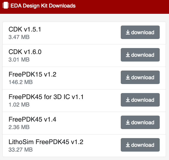
45nm/15nm/3nm NCSU FreePDK: NCSU has a variety of 45nm (FreePDK45) and 15nm (FreePDK15) design kits you can download from their website. If you really want to go to the leading edge, they have a 3nm PDK (FreePDK3) you can use for free.
Here is a complete list of available open source tools for almost any sub-field of electrical engineering that you are interested in. If you know of any more open source tools that you think is a must-have, leave a comment below.
There are plenty of resources available to do chip design but it is not always easy to setup these tools from scratch and start using them. For most tools, there is an online community that you can reach out for help.
TinyTapeout
TinyTapeout is a one-of-a-kind educational program that allows you to design a chip from the ground up using only open-source tools and even get it manufactured.
The founder of TinyTapeout, Matt Venn (X, LinkedIn), runs a course called ZerotoASIC that teaches ASIC design from the ground up and has an awesome YouTube channel. This is a perfect example of a practical-first education in chip design. It is designed to be accessible to university and high-school students and has affordable options to get chips manufactured.
Their chips used to be manufactured at eFabless, which unfortunately shut down recently. But now, TinyTapeout chips will be manufactured at IHP and can only be shipped within the EU and Switzerland. The chips manufactured at IHP are only on loan for your use, and you might be asked to return the chips after a period of two years. You can read the full details here.
Edit: Based on feedback from Matt, this chip loan restriction / export control is only for the next couple of shuttle runs and definitely not forever. Thanks to Matt for this clarification!
TinyTapeout represents a unique solution to actually make chip hardware for those who can avail of the manufacturing services.
Getting involved with open-source silicon
If you are interested in being part of the open source silicon movement, I suggest the following resources/conferences.
Free Silicon Conference (FSiC) — July 2-4, 2025, at IHP Electronics in Germany.
ORConf — September 12-14, 2025 in Valencia, Spain.
A step-by-step actionable guide to learning chip design
Although a lot of open-source tools are available, it can be challenging to find a starting point and make steady progress.
Here is a step-by-step actionable guide that teaches you how to pick a focus area, choose a design project, implement a design plan, execute it, and create documentation that will be useful throughout your career in chip design.