ABCs of Power Amplifier Classes: Class A
Design, operation and characteristics of the most linear amplifier class of all.
Hey, I’m Vikram 👋!
We begin down the path of power amplifier classes — the most basic one being Class A.
Please join our Discord server where have quite an active and vibrant RF community now. If you have any questions or comments, reply to this email. I’ll try to reply to everyone.
This post may be truncated in your email. Please click on the title to view the web version.
If you like this post, please click ❤️ on Substack. Subscribe to the publication, and tell someone if you like it. 🙏🏽
In this article, we will look at the Class A amplifier. It is a classical linear amplifier that delivers a faithful amplified version of the input signal.
Here's a quick summary of the foundational ideas discussed in the last post:
An amplifier requires an active device biased at a given current and voltage called its quiescent bias point or Q-point.
The input and output loads presented to the active device determine the amplifier performance.
Amplifiers are classified according to their output waveform.
There is always a trade-off between linearity and efficiency.
This article is part of a series on power amplifier classes of operation. You can jump to any one using the links below:
Class A Operation (this article)
In this post, we will discuss the following:
Common-source Class A amplifier
Choice of bias conditions and load line
Load network design
Peak and back-off efficiency
Design procedure
LNA vs. Class A PA
Read time: 11 mins
Common-Source Class A Amplifier
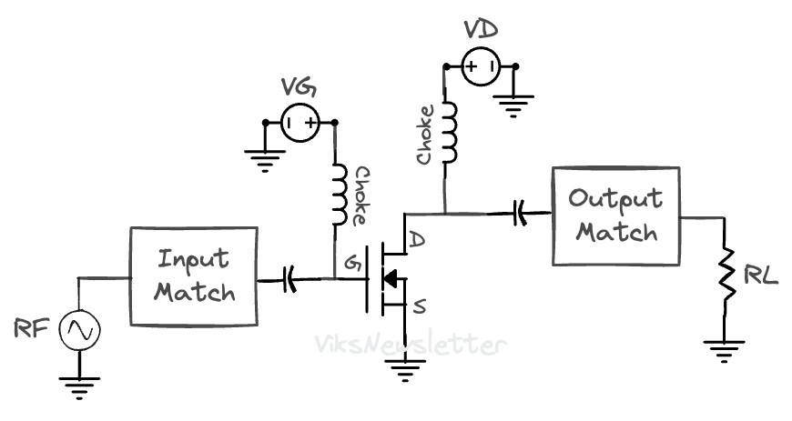
Class A amplifiers are ideal for applications where linear amplification is most important, not efficiency. A class A FET amplifier design shown below.
The circuit shows a common-source amplifier, where the "common" refers to the terminal to which gate and drain voltages are referred to. When source is the common terminal, any mention of gate or drain voltage really refers to the voltage between the gate-source or drain-source terminals (Vgs/Vds).
Here is an explanation of the schematic:
On the gate input side of the amplifier is a source resistance RS and a time-varying signal that requires amplification.
On the drain output side of the amplifier is a load resistance RL to which amplified power is delivered.
On both the input and output sides are matching networks that convert RS and RL into a complex impedance that is presented to the gate and drain terminals of the device.
There are bias generation circuits on the gate and drain that provide a gate voltage (VG) and a drain voltage (VD) to appropriately bias the FET device. They are feed through a choke inductor large enough to pass only DC through. DC blocking capacitors allow on RF signals to pass.
To make this circuit operate as a Class A amplifier, we need to bias the FET device so that the output waveform has as little distortion as possible.
Biasing and Load Line for Class A
Setting the quiescent bias point (Q-point) of the active device for Class A operation entirely depends on its current-voltage (IV) characteristics. The basis for doing so is stated as:
Choose Q-point so that instantaneous voltage and current in the device stays in quasi-linear (or active) region of operation.
From the IV space of the device, we can set voltages as follows:
Choose a drain voltage VD such that its instantaneous value during amplification:
will not exceed the maximum allowed drain voltage
will not put the transistor drain below knee-voltage, where it is primarily a voltage controlled resistor (keeps it in saturation)
Choose a gate voltage VG so that the instantaneous current:
will not exceed the maximum drain current supported by the device
will not drop to zero due to device entering cut-off
The result of these choices is that the Q-point often lies smack dab in the middle of the IV space that offers linear operation. VD is chosen to about half the maximum voltage tolerated by the transistor. VG is chosen so that the quiescent drain current is about half the maximum current supported by the device (Imax/2).
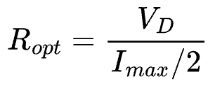
The next question is what kind of load should be presented at the output. If the drain voltage is VD and the drain current is Imax/2, then the optimum load resistance is
If the device has a non-zero knee voltage Vk, then the optimum resistance can be modified as
Load Network Design
Now that we know the optimum load that should be presented to the output of the transistor, we need to create a matching network that synthesizes this load.
It might be tempting to think that all we need is a conjugate match at the output. This is true if gain is the only metric we are looking to optimize. In the case of a Class A PA, our goal is to maximize the output power. For this we need a power match, which is what the calculation of Ropt is. It is quite unlikely that Ropt will be close to 50 ohms, and will therefore result in mismatch (poor return loss) at the output of the amplifier. We will revisit this point in a bit more detail later.
Load matching networks are usually implemented with lumped element or transmission-line based elements to manufacture the required impedances. These networks are inherently frequency limiting, and as a result, the amplifier tends to operate well in a finite bandwidth around a center frequency.
The losses in impedance matching networks also reduce the overall efficiency of the amplifier, and therefore a lot of effort is put into reducing the losses and improving the quality factor of passive components in power amplifiers.

Conduction Angles and Power Efficiency
The output current and voltage waveforms shown below will help calculate some important properties of Class A amplifiers. For all phases of the input sinusoidal signal, the transistor stays biased at its Q-point and conducting all the time.
The conduction angle for a Class A amplifier is 360°
The voltage and current waveforms are opposite in phase. This is consistent with the assumption that voltage goes up at the output terminal when current comes out of the device.
To find out how efficient a Class A amplifier is, we need to calculate how much RF power is generated for a given DC power. Instantaneous RF power is calculated as:
The average power over a full sinusoidal cycle is
So what are the amplitudes vo and io of the sinusoidal waveforms? Remember, we already put the quiescent bias point around the middle of the IV space. Our choice of VD is approximately half the maximum voltage supported by the device. This means that the AC signal can only swing to a maximum level of VD. So, let us set vo=VD.
Similarly, by choosing the DC current level at Imax/2, we can only expect the AC signal to swing another Imax/2 before it reaches it maximum possible value. So, let us set io=Imax/2.
The maximum possible average RF power is therefore only delivered when the input signal swings over the entire range of the allowed input values (not for smaller input signals). It can be expressed as,
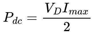
The DC power supplied is simply a product of the Q-point voltage and current.
Computing drain efficiency for a Class A amplifier is now easy.
The maximum efficiency achievable from a Class A amplifier is 50%
The drain efficiency is same as the power-added-efficiency (PAE) if the gain is high enough. But we begin to realize that half the supplied power is wasted in the pretext of linear amplification. This is why Class A amplifiers are not the preferred type for applications that rely on battery life. Having a 360° conduction angle continuously burns power in the active device, and lowers efficiency.
In reality, the presence of a non-zero knee-voltage (say Vk is 10% of Vmax of the device) in active device further reduces the maximum efficiency available to about 45%.
Backoff Efficiency
Notice that we mentioned that maximum efficiency is achieved only when the input drive signal is strong enough to occupy the entire allowable quasi-linear voltage range.
What happens when the input signal levels are reduced, or "backed-off" from the maximum level? This condition might occur if we simply do not want the amplifier to operate at its maximum power output all the time. Emission levels are regulated by the FCC and the radio transmitter is expected to function within those specifications.
Let us recalculate the average RF power output when the voltage and current swing are half the maximum allowed levels.
The output power drops to one-fourth the maximum power value. In terms of decibels, that is a 6 dB drop. This is a commonly used number in power amplifiers, and is called 6-dB backoff.
If you recalculate it, Class A efficiency in 6-dB backoff is 12.5%. This means that 7/8ths of the power is being wasted in the amplifier, and not being used for amplification. That is an unacceptably low level in power amplifiers and we will later see how this is improved in other classes of amplifiers.
The figure below explains intuitively why efficiency drops in back-off conditions. At high output power, the instantaneous power dissipates only occurs for a part of the signal cycle. As power level drops, the dissipation increases because the “always-on” transistor is constantly burning power without completely using the available DC power for amplification.

Design Procedure for a Class A Amplifier
Putting all these ideas together, how do you go about designing a Class A power amplifier? Here's a step-by-step approach:
Identify the active device: Determine the active transistor you will use. They are often engineered for power amplifier applications to deliver maximum output power. Ensure that your choice of transistor will meet your power needs.
Determine Q-point for Class A: Look at the current-voltage transfer characteristics of the device and identify the voltage and current range over which your signal will swing. Find a Q-point that ensures that the transistor is always operating in the quasi-linear region.
Determine optimum load: Once you determine the Q-point, calculate the optimal load that needs to be presented to the device. Most often this is a complex number and is a result of load-pull measurements of a device. For a given transistor, you will have an optimum load and bias conditions that will deliver maximum output power. If you are using a discrete transistor, it might be part of the datasheet. In integrated transistors, foundries and internal teams in companies perform measurements to find the optimal load and bias conditions.
Design load network: If your power amplifier is driving a 50 ohm load, then design a matching network that will transform 50 ohms into the optimum complex load required to power match the device. Make sure you use high quality passives to keep overall efficiency high.
Design input match network: The input match can be designed based on the principles of low-noise amplifier design. You can find the optimum input impedance to get the best gain using gain circles1, For a first cut design, a complex conjugate match to the input impedance of the transistor should suffice.
Verify the design: Once proper biasing and matching networks are designed, verify that the DC operating point, gain, output power and linearity are as expected from circuit simulations.
Difference between LNA and Class-A PA
We should understand the difference between LNA and Class A PA design. Both are linear amplifier designs but serve different purposes.
In LNAs, the main focus is high gain with low noise. This means that the voltage excursions on the device will not span a wide-range in the IV space especially because received signals are usually weak. This means that we will do just fine with a conjugate match at the device output for maximum gain from the transistor.
In Class A PAs, the focus is on sufficient gain with maximum output power and high efficiency. This means that we operate the device over its entire linear IV space by running the PA at high input signal levels. As a result, we need to have a power match based on an optimal load, which is different from a conjugate match.
As a result, Class A PAs might not always have the best output return loss because the main intention is to deliver maximum power and not entirely worry about the load impedance. RF systems often use circulators to avoid reflections back into the PA output. Whereas, in LNA design, there is a much higher emphasis on having good output matching.
The other difference is that the quiescent bias point in an LNA is relatively constant during the amplification process because the signal swing does not significantly alter the bias point. In that sense, the Q-point is quite static. In a Class A PA, the signal swing is large enough that the Q-point moves significantly throughout the process of amplification. The Q-point in this case is dynamic. Check out the discussion about static versus dynamic Q-points in an earlier article.
In the next article, we will see how conduction angle can be reduced to improve amplifier efficiency.
Stay tuned! If this article helped you, click the button below and leave a comment!
References
Inder J. Bahl, Fundamentals of RF and Microwave Transistor Amplifiers, Wiley & Sons, 2009.
Steve C. Cripps, RF Power Amplifiers for Wireless Communications, Artech House, 2nd ed.
This needs an article on its own.


Nice explanation...
As usual always great piece about rf blocks.