


First Impressions from 2025 ISSCC
"The Silicon Engine Driving the AI revolution," plenary talks and overall thoughts about the conference.

The view expressed in this newsletter are solely mine; they do not reflect the views or positions of my past, present or future employers, or any entities I am affiliated with. The content provided is for informational purposes only and does not constitute professional or investment advice. Always do your own research.
Attending ISSCC
The International Solid State Circuits Conference (ISSCC) is a forum for cutting edge research in various fields of semiconductor technology. Most talks from this conference are directed towards leading experts in various sub-fields of solid-state circuits, and are very information dense. This year, the acceptance rate for papers was approximately 25%!
In such conferences, there is no way one can sufficiently appreciate the intricacies of the all presentations made. The level of expertise required is simply too high. For example, an expert in memory will not comprehend all the details of high speed interconnect circuits.
Any reasonably technical attendee like myself needs a plan of attack to get the most of this conference. My strategy was to obtain two takeaways from every talk.
Problem: What is the problem they are trying to solve and why does it matter?
Results: What results did they get after solving the problem?
Between the problem and result(s) is the question of how they got the results. This is often technically intense, and does not add to the bigger picture. It only makes sense if you work in that sub-field.
With my framework, my hope was to develop a deeper appreciation for the state of the semiconductor industry without getting mired in the details. My purpose of attending a conference is to step back, survey the landscape, and then dive back into my own detailed technical work.
Annual Theme
This year’s theme was “The Silicon Engine Driving the AI revolution” and I joked online that this year’s conference might as well have been called AI-SSCC. The whole conference was understandably centered around AI. Most talks started with showing exploding transistor counts and compute FLOPS/TOPS, and how the industry needs to adapt to the growing need for compute.
I attended three days of conferences and a whole day forum on die-to-die interconnects. I will have to unpack a lot of the information slowly and reflect on what I learned. There is a lot of stuff I can write about from just attending this conference. If you would like to hear it, please sign up for a free or paid subscription using the button below. It supports my conference travel.
In this post, I provide my impressions from the conference as a whole, and tell you what I think of the plenary sessions.
Read time: 10 mins
Plenary Talks
Conferences open with plenary sessions, and this article should too. I like plenary talks only because it gives me a pulse on what the conference might be like, and what everyone is interested in. I usually don’t try to get too much technical learning out of them. There were four talks and each provided perspective in its own way — some more so than others.
AI Era Innovation Matrix
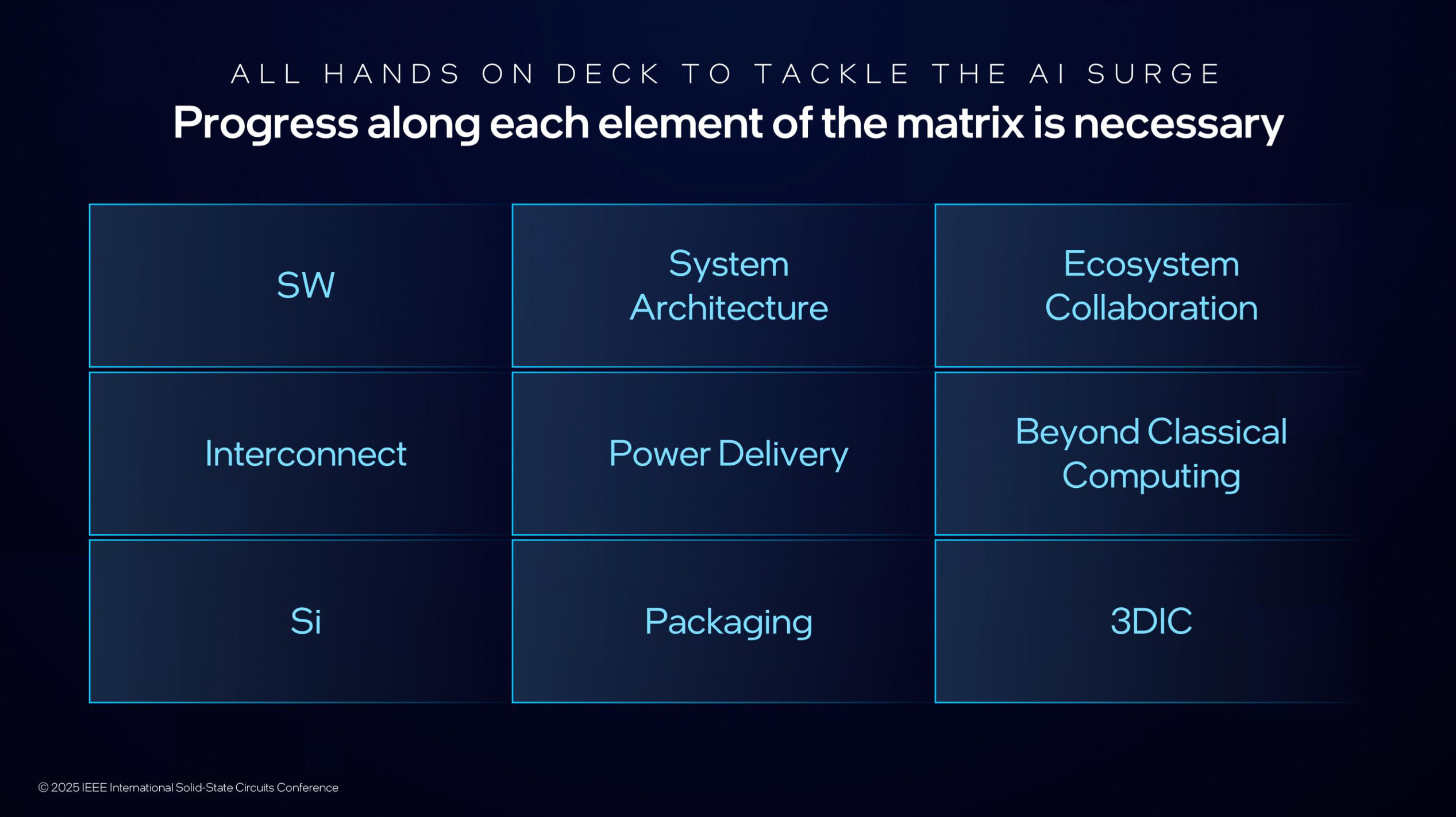
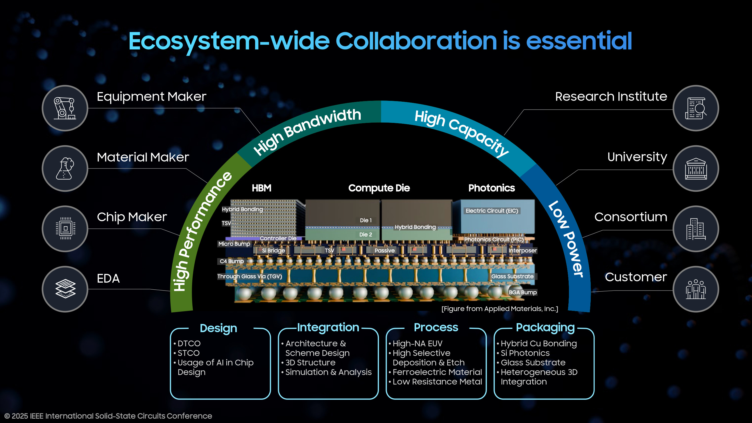
The first plenary talk was given by Navid Shariari, Intel’s Senior Vice President of Foundry Technology Development, who highlighted the missing pieces of the greater problem that needs innovation to solve. Pat Gelsinger was originally slated to give the plenary talk at this conference, but well, I guess plans change.
Shariari’s talk “AI Era Innovation Matrix” basically highlighted Intel’s capabilities to deliver across all domains for the future of AI, but specifically highlighted the need for increasing compute, disaggregation of silicon into chiplets, and advanced packaging for system integration. While he touched on power conversion and quantum computers, the primary message was the call for System-Technology-Co-Optimization (STCO). There were no remarkable announcements about possible the Intel split up, or anything along those lines; it was just a good old plenary talk.
AI Revolution Driven by Memory Technology Innovation
Samsung’s plenary talk was given by Jaihyuk Song, Corporate President and CTO, Device Solutions and was focused on memory technology innovation and the ‘Memory Wall’ of course, since memory is not scaling as fast as compute. The presentation was a nicely interleaved message around things that surround memory, like interconnects, packaging and in-memory compute.
By the end of the talk, my memory bingo card was full – HBM, 3D-NAND, Processing-in-Memory, hybrid bonding, CXL. Slides have the HBM roadmap, processing-in-memory, fancy DRAM implementations (4F2, 3D stacked DRAM), new NAND stuff with bonded VNAND), and cool packaging technologies. You should just watch the whole talk on YouTube for all the eye candy. I mean, just look at the picture below.
From Chips to Thoughts: Building Physical Intelligence into Robotic Systems
While these talks seemed rather run-of-the-mill plenary talks, Prof. Daniela Rus’ plenary talk on “Building Physical Intelligence into Robotic Systems” was a refreshing breath of fresh air compared to all the LLM training and interference stuff going on over the next couple of days. Prof. Rus is from MIT, and is also part of a MIT spinoff startup called Liquid AI that uses a different approach from the standard multiply and accumulate (MAC) operation approach in neural networks (the first of many alternatives to standard MAC I was to hear during the conference.)
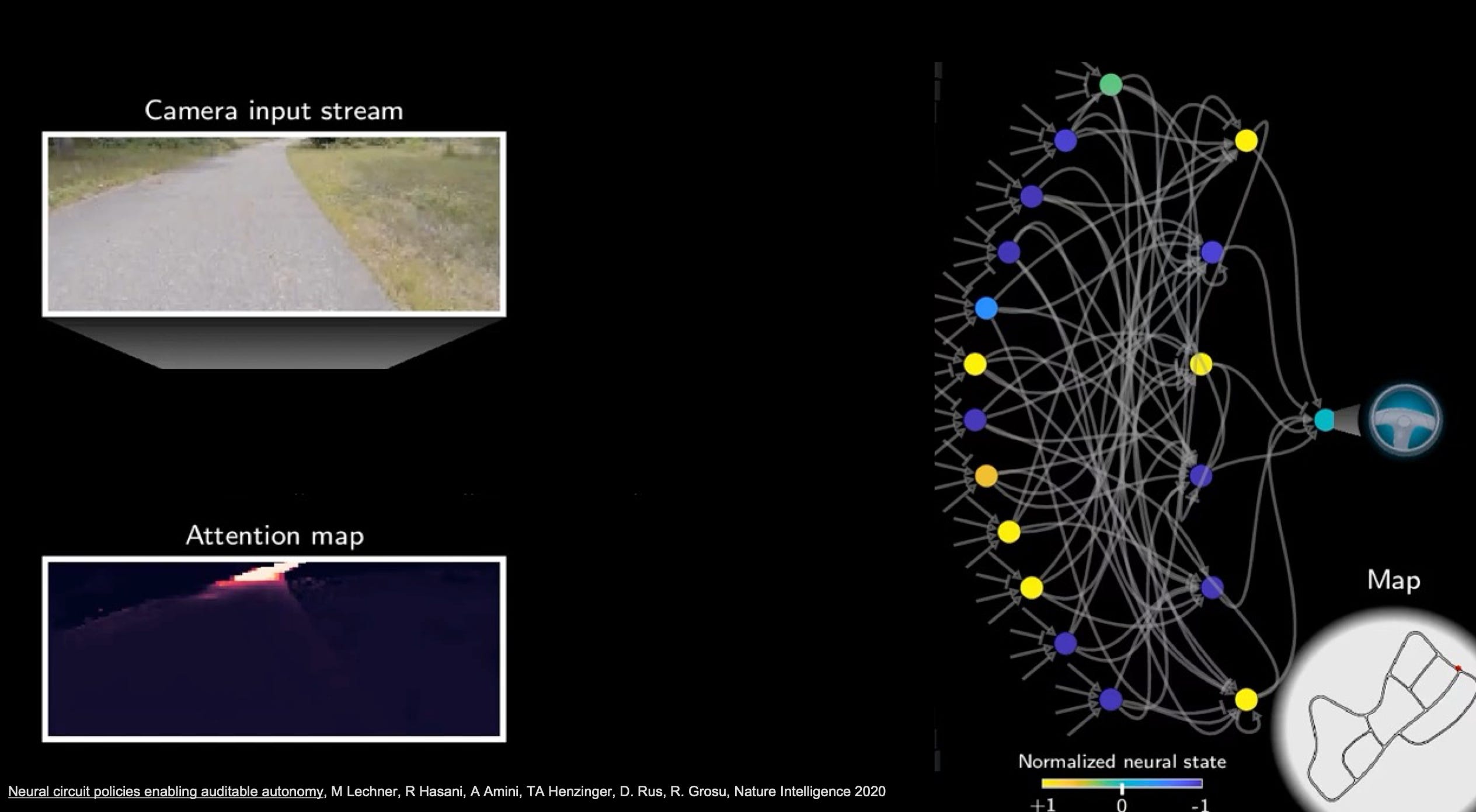
It turns out there is this nematode worm with just 302 neurons whose synaptic interactions are quite well understood by researchers that served as inspiration for this startup. They use a differential equation instead of the multiply-accumulate operation and call it a Liquid Neural Network. The premise is that this can be far more intelligent with fewer neurons, which makes it more efficient for robotic applications. Honestly, what impressed me most was the story-telling and the videos in the presentation. I’m sure the tech is impressive, but it just had a “wow” factor that appeals to human instinct.
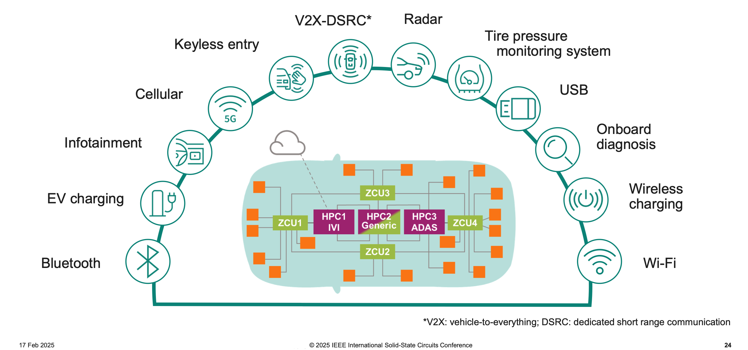
The Crucial Role of Semiconductors in the Software Defined Vehicle
The last plenary talk was by Peter Schiefer, President and CEO of Infineon’s Automotive Division about “The crucial role of semiconductors in the software-defined vehicle.” This is honestly as high level as a presentation can get. It’s one of those sessions where you hear a lot of words, but can’t tell someone what you understood. You can watch the whole thing yourself if you want to.
My key takeaway was this: automotive electronics uses every conceivable semiconductor technology there is. From high voltage devices like SiC for traction inverters, lower voltage but faster switching GaN for power conversion, high frequency InP or SiGe transistors for 77 GHz radar, legacy CMOS nodes for bluetooth, to leading-edge logic nodes for onboard CPUs and AI. What stood out to me was Infineon’s insistence that they will use RISC-V for their microcontrollers because who wants “IP lock-in” to ARM anyway. Look at all the kinds of functionality a car needs.
In the regular technical sessions, most of the excitement came from two domains:
Compute + Memory
Chiplets + Interconnects
Although there were a ton of other topics presented, these sessions were highly attended due to considerable relevance to the AI-centric semiconductor industry today.
Compute + Memory
Some of the most attended sessions at ISSCC were on processors, networking chips and AI training+inference chips. Here is a list of some big names that presented their work.
AMD: Zen 5 and Zen 5c processor architecture based on x86
IBM: Telum II processors for AI inferencing
Intel: Xeon 6 server chips
Samsung: Neural processing on Exynos system on chip (SoC) for mobile
SambaNova: SN40L AI training+inference chips
Broadcom: Tomahawk 5 — 51 Tbps networking ASIC
FuriosaAI: RNGD (Renegade) AI chips that use tensor multiplication, and had rumors around it that they were being acquired by Meta.
Most of these chips are the work of thousands of engineers all over the world. These presentations were surprisingly accessible given the complexity involved, and mostly focused on the type of architecture used and the resulting feature sets it provided.
There was also considerable interest in memory primarily because Intel and TSMC both presented SRAM using nanosheet transistors (also called ribbonFET or gate-all-around). This is because it is a demonstration that 18A is functional, and TSMC has competition at the leading edge.
The added surprise also seems to be that Intel's 18A is close to TSMC's 2nm from pure SRAM density numbers, although SRAM alone does not tell you all that you need to know about the performance of a process node. Intel's 18A is also the first node to use back-side power delivery through PowerVias. TSMC's 2nm node does not have this feature yet. This lead some to believe that Intel might actually be ahead in the nanosheet transistor era. Intel announced that 18A is ready for production runs in 2025 with chips like the Panther Lake being the lead product on the node.
Disaggregation + Interconnects
Disaggregation is the future. We want to break up one big chip into smaller pieces called chiplets, and for good reasons too. Advanced nodes using nanosheet transistors will benefit logic chips in terms of speed, but they are also ungodly expensive. Other parts of the SoC such as power and input-output (IO) does not need this complexity, and will benefit from cheaper nodes.
The other nice benefit of using chiplets is that you can use a mix of chips from different vendors to build an SoC — like you would go on DigiKey today to buy parts for a system built on PCB. These chips would then talk to each other using high speed interconnects, and behave as though they were a single monolithic chip.
In fact, when the presenter from Broadcom was asked about the next generation of its network ASIC, Tomahawk 6, he mentioned it was going to be chiplet based, and that it is not possible to stay monolithic past Tomahawk 5. I regarded that as a sign for where we are headed — heterogenous integration.
To make sure that chips from different vendors can talk to each other, you need an interconnect standard like Universal Chiplet Interconnect Express (UCIe). Think of these as circuit blocks you would put at the periphery of every chiplet, so that it can speak the same language as other chiplets. There were many talks on UCIe and vendors such as Cadence and Synopsys are developing IP blocks that meet all the required specifications, which can be dropped into any chiplet design.
Intel demonstrated one such chiplet-based design for AI inferencing. Their approach is to standardize the bump patterns where chiplets will land on the passive silicon die, what they called a chiplet slot, and then drop in chiplets from both TSMC and Intel chips into them. They showed a 20 chiplet system put together like lego blocks on a substrate that was capable of AI interference — proof that disaggregation works.
And while it worked, my skepticism comes from the overhead of putting UCIe peripherals on each die. A disaggregated system needs die-to-die interconnect drivers on every chiplet, which was not necessary when it was a monolithic SoC. Thus, part of the chiplet is consumed by the associated fixed silicon cost for peripheral connectivity.
For the economics to work out, the use of legacy manufacturing nodes and added cost of packaging should be lower than the cost of a monolithic die. Chiplet economics, or when to use chiplets (and when not to) was part of the all-day forum I attended on die-to-die interconnects. I’ll get to that in a future post.
You can earn a 1 month paid subscription by recommending just two people to this publication using the button below.
Would love to hear more about recent progresses on 3D interconnects (more products in market recently) and the effects it has on reimagining design - integration - packaging co-optimisation. This actually requires to go for System first approach, model down to every interconnects for power, performance (latency limiter) and reliability.
Good event