Understanding Energy Bands in Semiconductors
Valence and conduction bands, forbidden and Fermi energies, density of states, Fermi-Dirac statistics.
This is the first article of The Joy of Semiconductor Devices series — a collection of posts that explains the inner workings of semiconductor technology from first principles in an accessible manner.
Here are the topics covered in this post:
Semiconductors at equilibrium
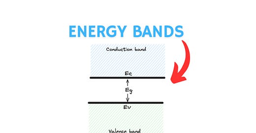
Valence and conduction bands in semiconductors
Forbidden energy gap / Bandgap
Density of States
Fermi-Dirac statistics and Fermi level
Read time: 10 mins
Semiconductors at Equilibrium
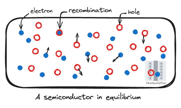
If you closely look at a piece of semiconductor in thermal and electrical equilibrium at room temperature, you will observe random motions of electrons along every direction. Electrons are usually held in place by the electrostatic forces from atoms in the material, or in other words, by the attraction between positive charges in an atom’s nucleus and negative charges in the electrons. The atoms in a material often have a regular formation, and in semiconductors they are assembled into grid-like structures called a crystal lattice.
By the nature of a semiconducting material, some electrons are knocked loose from the crystal lattice by absorbing energy from the thermal sources such as ambient temperature and they are now free to move around the crystal lattice allowing a limited amount of conduction.
The spot in the crystal lattice that now has a missing electron is called a hole, and is positively charged. Since the formation of a free electron and hole happen together, they are called electron-hole pairs. When an electron occupies the empty spot in the crystal lattice (a hole), it is called recombination and the positive hole charge is neutralized by the negative electron charge. However, the spot that the electron left behind to perform recombination now forms the hole. Thus, you can envision that holes move in a direction opposite to electrons. In a semiconductor in equilibrium, this happens in all directions and there is no net charge transport in any direction; the semiconductor remains electrically neutral.
Energy Bands in Semiconductors
In the classical Bohr model of the atom, electrons have different orbits around a nucleus consisting of protons and neutrons which is an easy way to visualize things. This has largely been replaced by a quantum mechanical view of an atom where each electron is located in discrete orbitals and has an energy level associated with it. Outer orbits have higher energies, and for an electron to make a transition to it from a lower orbit, it needs to be given a discrete amount of energy, usually via optical, electrical, mechanical or thermal sources. In practice, atoms don’t exist in isolation. So we have to modify our world view a little bit.
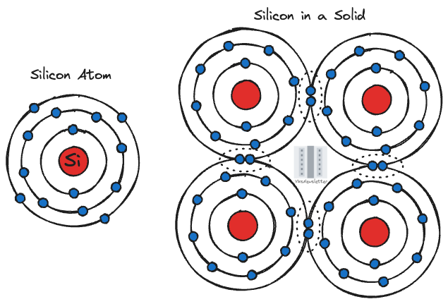
In a solid material such as a semiconductor, there are a large number of atoms present. Silicon for example, shares the four electrons in its outer orbit with neighboring atoms forming what is known as a covalent bond. It becomes immediately apparent that an electron is not alone, but is influenced by all the electrostatic forces from the neighboring atoms and other electrons.
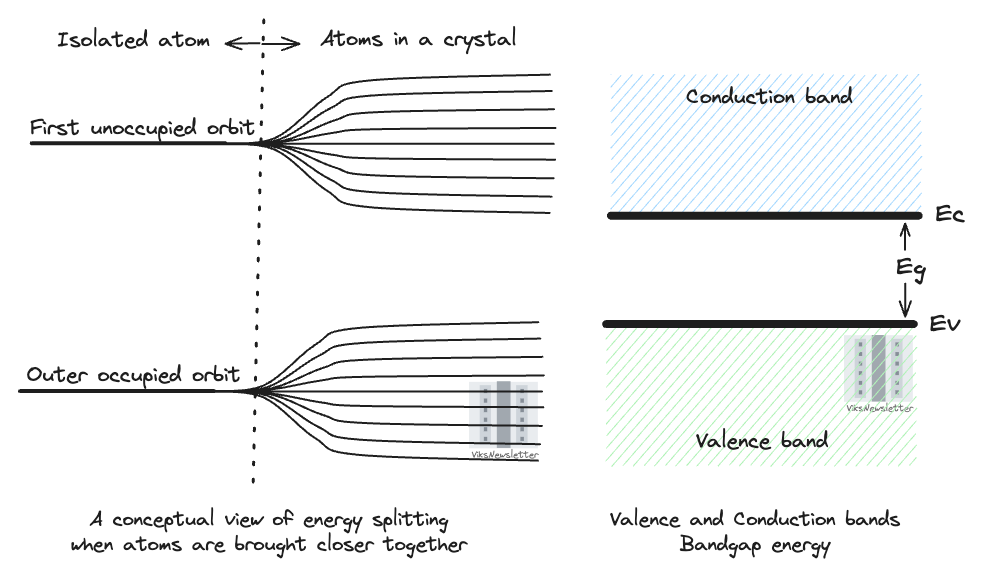
For simplicity, consider the example of two silicon atoms brought together. While their electron orbit energies are same when considered separately, something different happens when they exert an influence on each other. The energy levels of their orbits split into slightly higher and slightly lower levels. This is due to the Pauli exclusion principle which imposes that no two electrons can occupy the same quantum state at any time. The splitting of energy levels provides exclusive quantum states for electrons in the two atoms, thereby satisfying the exclusion principle.
When a large number of electrons are brought together, a large number of closely spaced energy levels are formed as a result of splitting thus forming an energy band. In reality, how this happens is far more complicated, but it is enough here to understand why we will talk exclusively in terms of energy bands from now on and not just energy levels in semiconductors.
While many energy bands exist in a semiconductor material, we are concerned with two of them.
Valence Band: Electrons present in the outermost orbit of the atom of a semiconductor are called valence electrons and are responsible for forming covalent bonds between atoms. These electrons are not free to move because they are held in place by the electrostatic force of the atoms that surround them. In terms of energy bands, it can be defined as
Valence band is the highest occupied energy band in a semiconductor at absolute zero temperature (0 Kelvin).
Conduction Band: When electrons in the valence band are provided sufficient energy from thermal, electrical or optical sources, they can accumulate enough energy to transition to the conduction band where they are unconstrained by the electrostatic forces of atoms and free to conduct electricity. In terms of energy bands, the conduction band can be defined as
Conduction band is the lowest unoccupied energy band in a semiconductor at absolute zero temperature (0 Kelvin).
Forbidden Energy Gap or Bandgap Energy
Whenever electrons move from the valence band to the conduction band, they do so in a discrete fashion. They accumulate energy to jump to a different energy level without going to any of the intermediate energy levels. This is a consequence of quantum mechanics when dictates that electrons can occupy only discrete energy levels. Any of the intermediate energies constitute the forbidden energy gap (Eg) which no electron can occupy.
This forbidden range of energies is also called the bandgap of the material and is specified in units of electron-volts (eV). This is an important figure of merit for a conductor, and one that you will often come across when discussing different materials used for constructing transistors.
One electron-volt is the energy gained by an electron when its electric potential is increased by one volt. The charge on an electron is -1.6 x 10^-19 Coulomb, and when one volt is applied to it, its energy gain is 1.6 x 10^-19 Joules, which is 1 eV. When talking about energies of electron orbits, they are usually negative values due to electron charge, but differences in band energy levels are positive numbers.
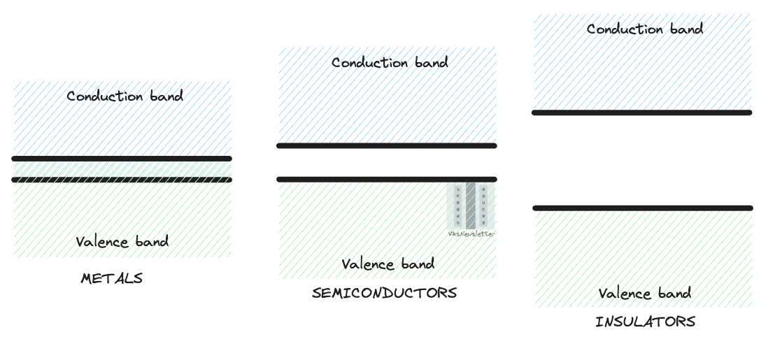
Conduction in a material only occurs when the electrons from the valence band are moved to the conduction band. In metals, the conduction and valence bands overlap and electrons are readily available for conduction without the need for external influence. In insulators, the bandgap energy is usually so large that it is difficult to move electrons from the valence to conduction band for conduction. In such cases, electrons stay confined to their atomic crystal structure without being able to move, and hence have insulating properties.
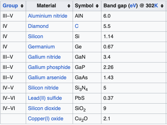
Semiconductors usually have a small bandgap (~1 eV) which implies that they can be made to conduct electricity with ease with some amount of external help. Large bandgap energies (~ 3 eV) are also a feature for semiconductor devices such as gallium nitride and silicon carbide because these materials are capable of withstanding a lot of voltage and current, and are typically used for high power voltage conversion applications in electric vehicles, energy infrastructure and industrial electronics. Bandgap energies of some popularly used materials are shown below (source: wikipedia; see here for a more detailed list).
Density of States
We looked at how energy levels split when a collection of atoms are present. In the valence or conduction band, there are now a large number of closely spaced energy levels. But there is no reason to assume that these split energy bands are evenly spaced from each other within the range of energies in any band. They can be closely spaced in some energy levels but sparse in others. We can actually talk about how dense these energy levels are around any given energy level using the metric of density of states.
Density of states is the number of energy states per unit energy.
We visualized density of electron states along one axis for the above definition. In reality, the energy distribution is in three dimensions as we will see in more detail later. Thus, the density of states is also normalized per unit volume. Here’s another explanation that is more intuitive than the first, although it is still a loose definition.
Density of states describes how electrons populate the energy levels of the band they reside in.
Remember that density of states is only meaningful in energy bands where electrons can actually exist, like valence and conduction bands. The density of states in the forbidden energy gap is zero, since no electrons can occupy those energy levels.
Fermi-Dirac Statistics and Fermi Energy
Although we looked at how the energy levels split up when many atoms come together, and how these energy levels are distributed within any given band (valence or conduction) via density of states, there is no guarantee that an electron is actually present in any given energy level at a time instant. We can only talk about the probability that we can find an electron in any given energy state. Remember this is quantum mechanics we are talking about. Nothing is deterministic.
The probability of finding an electron at any given energy E is given by Fermi-Dirac distribution function, and is so fundamental that we will show the equation below.
where F(E) is the probability, k is Boltzmann’s constant, E is energy and EF is the Fermi energy. Fermi energy (or level) is a key concept that we will repeatedly use while drawing energy band diagrams of semiconductor devices.
Fermi energy is the energy level in a semiconductor material where the probability of finding an electron is 50%.
In an intrinsic semiconductor (meaning without doping impurities which are usually added to alter the properties of a semiconductor), the Fermi energy is exactly between the valence and conduction bands. But isn’t that in the forbidden energy gap? Shouldn’t the probability there be zero since no electrons can exist? No, the probability of finding an electron is non-zero, but we will not find any electrons there since the density of states is zero.
It will become clearer when we actually try to calculate how many electrons are present in a unit volume of semiconductor, which is a key quantity we will need to determine the flow of current through it. To find the electron density, we multiply the density of states, N(E), with the probability of finding an electron at that state, F(E), and add up the contributions over the range of allowed energies in the band. Converting english to math,
n(E) is the electron density, N(E) is the density of states, F(E) is Fermi-Dirac probability distribution and Emax is the maximum energy level in the band.
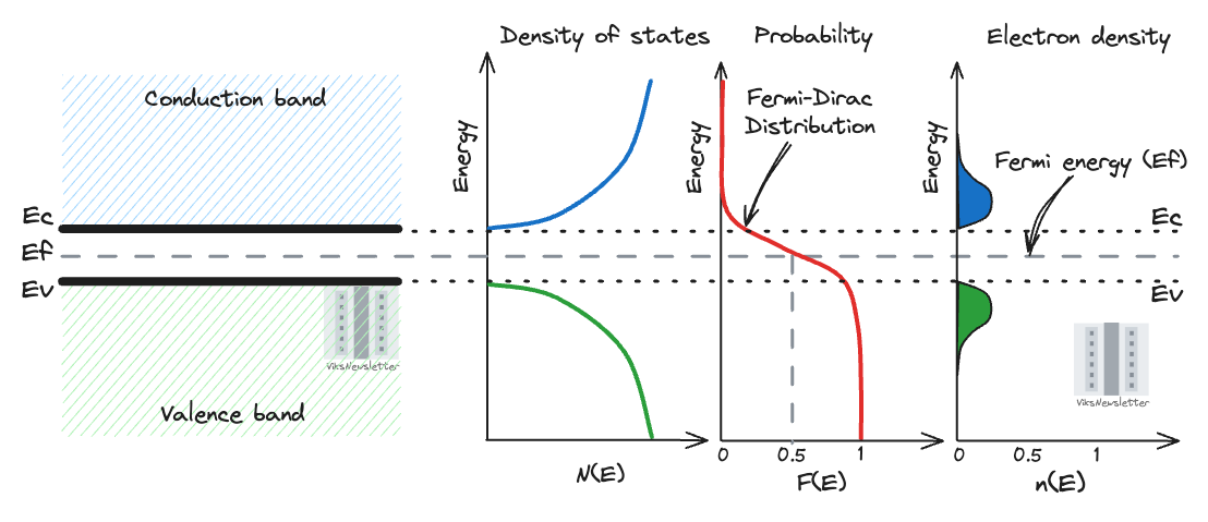
Let’s understand these graphs a bit more.
We can see that the Fermi energy EF is exactly in the middle of the forbidden energy gap. That is because this is an intrinsic semiconductor.
The density of states is lowest right at the edge of the bands, but there are more split energy levels that electrons can occupy at higher levels.
The Fermi-Dirac distribution shows the probability of finding an electron at any given energy level. The red line shown strongly depends on temperature, where the slope of the transition gets steeper at lower temperatures. At Fermi energy, the probability of finding an electron is 0.5, or 50%.
The electron density as a function of energy is a product of the density of states and Fermi-Dirac distribution. If we calculate the area under the little humps in the valence and conduction bands, we will find the total electron density in a unit volume of semiconductor. This is what the integral sign in the last equation means.
Here is why Fermi level is so important in solid state physics and especially in semiconductor junction behavior.
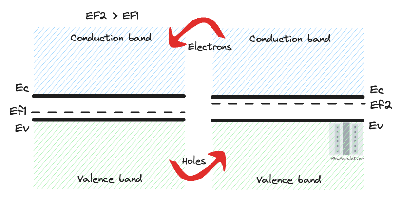
Whenever two materials with different Fermi levels are brought into contact with each other, electrons will flow from the material with higher Fermi level to the one with lower Fermi level (and holes from lower to higher Fermi levels), till their Fermi levels are the same, to achieve equilibrium.
This is an important fact we will use in learning to draw energy band diagrams for various semiconductor materials. In the process of aligning Fermi levels, the conduction and valence bands will bend to accommodate a constant Fermi level, and this will explain a lot of the behavior observed in semiconductor junctions, which we will discuss later.
Read the next post.
Semiconductor Doping, Electron Affinity, Work Function and Anderson's Rule
This article is part of The Joy of Semiconductor Devices series — a collection of posts that explains the inner workings of semiconductor technology from first principles in an accessible manner.
If you like this post, please click ❤️ on Substack and subscribe to the publication.
Refer just 2 people to this publication, and get 1 month of paid subscriber benefits!
Join our Discord community and get in on the discussion!
The views, thoughts, and opinions expressed in this newsletter are solely mine; they do not reflect the views or positions of my employer or any entities I am affiliated with. The content provided is for informational purposes only and does not constitute professional or investment advice.




Here is a statement from the text that I have issues with, regarding the Fermi level
"No, the probability of finding an electron is non-zero, but we will not find any electrons there since the density of states is zero."
That part of it "we will not find any electrons there since the density of states is zero" implies absolute certainty i.e. a probability of 1. The part that the Fermi level corresponds to a probability of 1/2 suggests lack of an absolute certainty.
I think the above statement has to be reformulated.