


Semiconductor Doping, Electron Affinity, Work Function and Anderson's Rule
Controlling the energy levels in semiconductors, and learning to draw energy band diagrams from intrinsic material properties.

This article is part of The Joy of Semiconductor Devices series — a collection of posts that explains the inner workings of semiconductor technology from first principles in an accessible manner.
Doping semiconductors with impurities
N-type and P-type Semiconductor
Energy levels in the presence of impurities
Adjustment of Fermi Level
Electron affinity and work function
Anderson’s rule
Example of silicon P/N type semiconductors
Example of dissimilar materials
Read time: 9 mins
Here is the previous post in the series.

Doping semiconductors with impurities
In the last post, we left off by showing two materials with different Fermi energies. How can a material have the same valence and conduction band energies but have different Fermi energy levels? In semiconductors, the Fermi energy can be adjusted to various levels within the forbidden energy gap by introducing impurities into the silicon crystal structure. The process of adding impurities to a semiconductor is called doping, after which it becomes an extrinsic semiconductor. We mentioned earlier that the outermost orbit in a silicon atom uses four electrons to form covalent bonds. This number is key to understanding how added impurities will behave in a silicon crystal.
N- and P-type semiconductors
Consider the case of adding an atom (such as arsenic) which has five electrons in its outer most orbit, which are generally elements in Group V of the periodic table. When this impurity atom inserts itself into the crystalline structure of silicon, it uses only four of its five available electrons. This leaves the fifth electron loosely bound to the impurity atom. Even a little bit of energy from ambient thermal sources called ionizing energy is sufficient to separate the extra electron from its host atom, which is now free to move and contribute to conduction.
In a sense, the impurity atom has “donated” a negatively charged electron to conduction and has itself become positive in the process. Such impurity atoms are called donor atoms, and the resulting material is said to be an n-type semiconductor. Though positively charged, donor atoms are immobile unlike the electrons they donate for conduction.
Since electrons mostly contribute to conduction in an n-type semiconductor, electrons are called majority carriers, while holes present in an n-type semiconductor are called minority carriers.
If we add an impurity atom with only three electrons in its outermost orbit (a group III element such as boron), it “accepts” an electron from the silicon atom when forming covalent bonds while leaving a positively charged hole in its place. Therefore, such impurities are called acceptor atoms, and the resulting material is a p-type semiconductor. Acceptor atoms after ionization become negatively charged due to the acquired electron, and are immobile due to their place in the crystal structure. Since holes mostly contribute to conduction in an p-type semiconductor, holes are called majority carriers, while electrons in a p-type semiconductor are called minority carriers.
Energy levels in the presence of impurities
Since we added an impurity and broke the periodic crystal structure, the forbidden energy gap is not so forbidden anymore. The impurity atoms we added will introduce their own energy levels in the band gap. The figure below shows the relative energy levels of some popular dopants used in semiconductors.
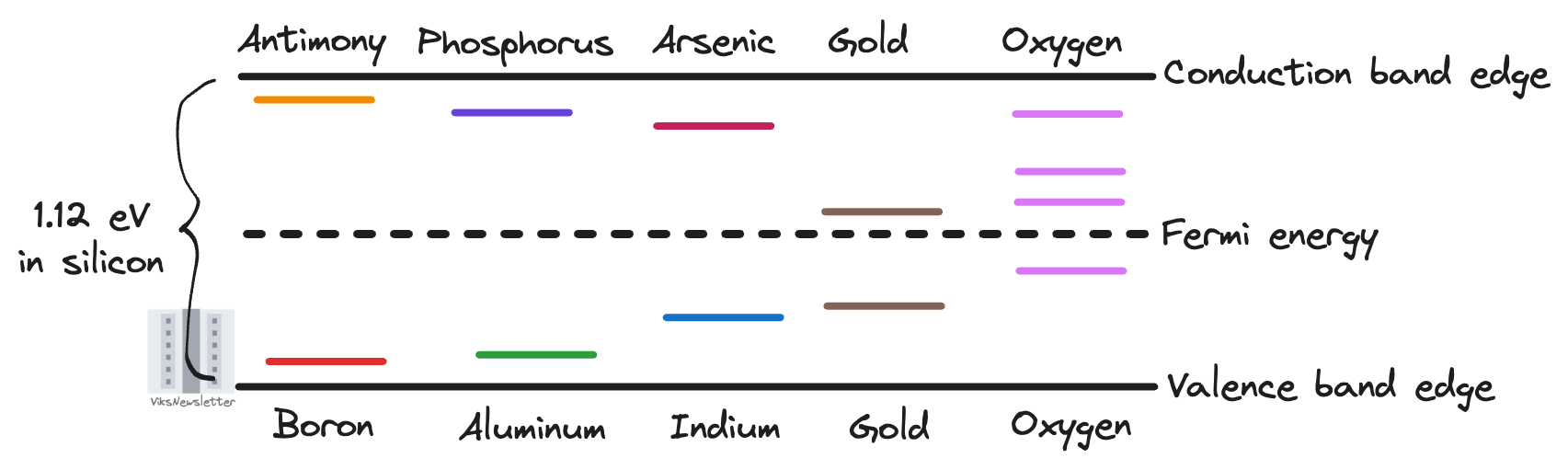
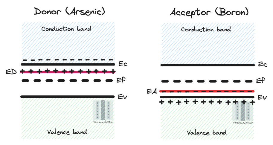
Let us clarify what each of these lines in the bandgap actually represent. When an element such as arsenic donates its electron, the donated electron moves to the conduction band, and the positively charged donor arsenic atom now occupies the indicated energy level (ED) just below the conduction band edge.
Similarly, when boron accepts an electron, it creates holes that can move within the valence band resulting in conduction. The negatively charged acceptor boron atom then occupies the energy level (EA) indicated just above the valence band edge.
There are some elements such as oxygen and gold that present multiple energy levels within the bandgap, and are useful for specific applications like controlling how long it takes for recombination effects between majority and minority carriers to take place in semiconductors. We won’t get into these for now, but I just wanted to highlight that an element may present multiple energy levels for the sake of completeness.
Adjustment of Fermi Level
In its intrinsic state, the semiconductor has a Fermi energy level in the middle of the bandgap. It can be moved away from the middle by doping it with either donor or acceptor atoms.
Doping with a donor atom (more outer electrons than semiconductor) will cause the Fermi level to shift towards the conduction band.
Doping with an acceptor atom (less outer electrons than semiconductor) will cause the Fermi level to shift towards the valence band.
The extent to which the Fermi level shifts towards the conduction or valence band depends on the concentration of atoms used in doping the semiconductor.
If more donor or acceptor atoms are used, then the Fermi energy moves closer to the conduction or valence band, respectively. Although there are ways to calculate the Fermi energy given a certain doping concentration, it is sufficient to understand this effect qualitatively for now.
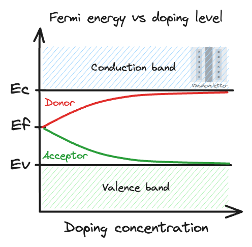
These approximate graphs are valid as long as the doping concentration is not so high that the Fermi energy approaches the valence or conduction bands. In such cases, the semiconductor is said to be degenerate and various higher order, complicated effects kick in.
In essence, this is how the properties of devices made from semiconductors are controlled, and is an essential step to getting the right performance from the solid state device. We will see more of this when we look at junctions formed between similar and dissimilar materials.
Electron Affinity and Work Function
While we now understand that valence band electrons can gather energy and transition to the conduction band, what happens if those electrons are given even more energy? With additional energy, the electrons from the conduction band can entirely leave the material and enter free space. Depending on the source of energy, this phenomenon is named differently: Thermionic emission (with heat), Field emission (with electrostatic field), Photoelectric effect (with light).
Based on this, we can define two quantities:
Electron affinity is the amount of energy released when an electron in vacuum is inserted into the conduction band of a material.
Work function is the amount of energy required to remove an electron from the Fermi level to vacuum level.

Imagine an electron hanging out in free space. Electron affinity is the amount of energy would it take to remove the electron from free space and insert it into the conduction band of a material. Electron affinity is fundamentally a property of a material, and depends on its atomic structure.
Work function is the amount of energy it takes to take an electron having Fermi energy and place it in vacuum. Fermi level is material dependent and a function of how many dopant impurities are present, and hence work function also depends on these factors.
We will use these quantities to establish an energy reference levels as we will see next, to eventually draw energy diagrams.
Anderson’s Rule
Before we go any further into constructing band diagrams for semiconductors, we need to understand Anderson’s Rule, which states,
When constructing an energy band diagram, the vacuum levels on either side of a semiconductor junction should be aligned.
This means that simply knowing bandgap and Fermi energies is not sufficient to draw energy band diagrams. The electron affinity of the materials involved is required to set the reference level for the energies involved. This rule is better explained with an example.
Example 1
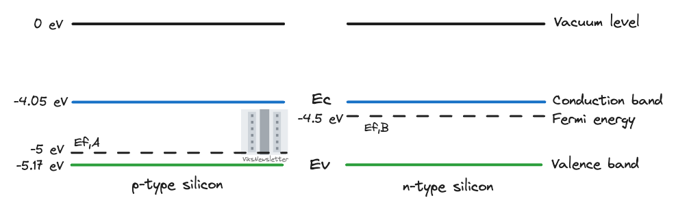
Assume that p-type silicon and n-type silicon are next to each other, but not contacted. The intrinsic properties of silicon and the Fermi levels for p- and n-type silicon have the following energies:
Electron affinity for silicon = 4.05 eV
Band gap of silicon = 1.12 eV
Fermi level of p-type silicon = -5 eV
Fermi level of n-type silicon = -4.5 eV
Anderson’s rule dictates that we first line up vacuum levels, and then the electron affinity tells us where the conduction band is. Since both materials are silicon in this example, the conductance band energy of both p- and n-type silicon is the same, -4.05 eV, which is calculated from electron affinity. Given the band gap of silicon, we can find the valence band levels for both materials as -(4.05 eV + -1.12 eV) = -5.17 eV. Then we have the Fermi energies for both materials readily available. The energy levels of these two uncontacted materials looks like the picture below.
When these materials are contacted, electrons will flow from n-type silicon to p-type, and holes will flow from p-type to n-type, till their Fermi levels equalize. We will draw those band diagrams when we talk about p-n junctions.
Example 2
Let’s get more crazy. For the sake of being oddly specific, and also practical, say that we place p-doped Aluminum-Gallium-Arsenide (p-AlGaAs) and n-doped Gallium-Arsenide (n-GaAs) next to each other. These dissimilar materials have some remarkable properties as we will see later. For now, we just want to look at some energies. Here are the energy levels related to each type of material:
Electron affinity
AlGaAs = 2.62 eV
GaAs = 4.07 eV
Band gap
AlGaAs = 2.16 eV
GaAs = 1.43 eV
Fermi level of p-AlGaAs = -4 eV
Fermi level of n-GaAs = -4.4 eV
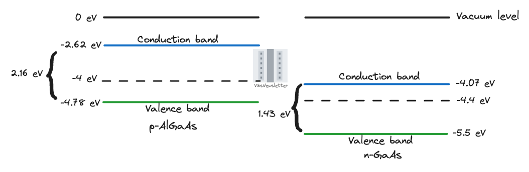
We first have to establish the conduction/valence band and Fermi energy levels for each material. From a 0 eV vacuum level, we can calculate them as below.
For AlGaAs, the electron affinity is 2.62 eV, and the valence band will be a bandgap away from that, or at -(2.62+2.16) eV = -4.78 eV. The Fermi level is at -4 eV, or closer to the valence band because it is a p-type doped semiconductor.
For GaAs, the electron affinity is higher at 4.07 eV. The valence band will be a bandgap away again, or at -(4.07+1.43) eV = -5.5 eV. The Fermi level at -4.4 eV is closer to the conduction band because it is an n-type doped semiconductor.
This represents an interesting case because the Fermi level of the n-type semiconductor is actually below that of the p-type. This did not happen in our silicon example because the electron affinity for both the p- and n-type materials were the same. This can actually happen when using dissimilar materials and is why we need to start from aligning energy bands with electron affinity as a reference using Anderson’s rule.
By cleverly choosing materials and adjusting Fermi levels, we will later see that we can engineer heterojunctions that provide incredible levels of mobility because the properly engineered energy levels allows us to trap a bunch of electrons in a ‘quantum well.’ This gives rise to the remarkable properties of Gallium Arsenide, Gallium Nitride or Indium Phosphide transistors that simply don’t occur in silicon transistors.
You can earn a 1 month paid subscription by recommending just two people to this publication using the button below.
Join our Discord community and get in on the discussion!
The views, thoughts, and opinions expressed in this newsletter are solely mine; they do not reflect the views or positions of my employer or any entities I am affiliated with. The content provided is for informational purposes only and does not constitute professional or investment advice.
loved the examples!
At first I thought semiconductor doping would be a new term for false claims on how much it costs to train a model :)