A Guide to Noise Sources in MOS Transistors
Learn how thermal, flicker, shot and induced noises in MOS transistors contribute to the generated noise spectrum, with each having its own frequency dependence.
Hey, I’m Vikram 👋 and thanks for reading!
Connect with me on LinkedIn/X and reply to this email with your feedback. I highly recommend joining the Substack chat.📝
If you like these articles, please let others know. Word of mouth helps grow this newsletter! 🙏
Noise is the great limiter. Without it, we could communicate over arbitrarily large distances while consuming almost no power. Unfortunately for us mere mortals, noise is here to stay, and we need to overcome it.
In this article, we look at the sources of noise in MOS devices. You will learn:
Power spectral density
Noise in a resistor
Thermal noise
Gate noise
Flicker noise
Induced noise
Shot noise
Let’s dive in!
Power Spectral Density
Let's look at current flow in a wire when a battery is connected to it. At room temperature, you will have an average current flow depending on the wire resistance. There will also be fluctuations of current at every point of the wire due to random motion of electrons. You cannot predict the instantaneous current at any point in time because it is completely random. This noise from the random motion of electrons can only be represented by its average power, which you get by squaring the noise and averaging over time.
Fluctuations can happen fast or slow since it is completely random. Hence, the noise power spectrum can have a wide range of frequencies. To find the power at any frequency, we run the time domain signal through a filter bank as shown in the figure below. Each filter has a different center frequency and an ideal 1-Hz bandwidth. At the output of each filter, we measure the average power. The result is called the Power Spectral Density (PSD) of the noise signal, whose unit is volts-squared per hertz if its voltage noise or ampere-squared per hertz if it is current noise.
Noise in Resistors
The PSD of noise in a resistor R is given by 4kTR, where k is Boltzmann's constant and T is absolute temperature in Kelvin. It is often called white noise because like white light, it contains all the frequencies with equal power levels.
If we were to calculate the area under the white noise to find total noise energy, we get an impossible result. Infinite energy from finite ambient temperature. Well, turns out that noise is not that white after all, and the PSD starts to fall off at frequencies over a terahertz.
To avoid this confusion, it is easier to calculate noise energy in a 1-Hz bandwidth. This means that 4kTR is the noise power in a resistor when a 1 Hz bandpass filter is applied at any frequency below a terahertz. To make it easier for electrical engineers, take the square root of the average noise power and represent it as a root-mean-square (RMS) noise voltage expressed in Volts/√Hz.
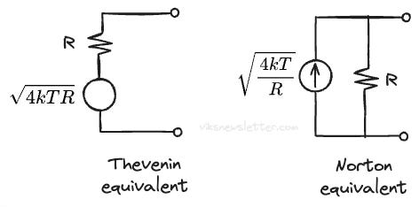
Square-root of hertz is a strange unit, but we live with it because the numerator is in volts, and lends itself to circuit analysis nicely. Given any circuit with a noisy resistor R, you can immediately replace it by a noiseless resistor with a noise voltage or noise current. The Thevenin and Norton representations shown below prove quite useful in circuit analysis. If noise voltage is expressed in V/√Hz, noise current is A/√Hz. For this rest of this article however, we will stick to representing noise with PSD.
Noise in MOS Transistors
There are a variety of noise sources in MOS transistors and we will discuss each one of them. It is helpful if you have a basic understanding on MOS transistor operation.
Channel Thermal Noise
The path between the source and drain terminals in a transistor is called the channel. This is where the current conduction actually happens when the gate voltage is above a certain threshold. The motion of electrons through this channel is one of the predominant sources of noise in a transistor, whose current noise PSD at the drain is given by
where gd0 is the output conductance (inverse of resistance) of the transistor when zero volts is applied to source and drain1. 𝛾 is the white noise gamma factor (or excess noise coefficient) with a value of 2/3 for transistors whose gate length is sufficiently large (>1 micron).
As the gate length of the transistor shrinks below 1 micron, the value of 𝛾 goes up to even 2 due to noise contributions from parasitic resistances and other effects that are unique to transistors with small gate lengths. The value of 𝛾 is usually determined by measurements for each particular technology node.
The figure below shows the channel thermal noise as a function of frequency, gate-source voltage, and drain-source voltage, for different gate lengths (from 0.25um to 1um). The figures are only qualitative, but intended to highlight the following about channel thermal current noise:
It is higher for small transistor gate lengths due to increased parasitic resistances
It remains relatively flat with frequency showing that it is "white" in nature
It increases with gate-source voltage
It is relatively insensitive to drain-source voltage because the pinch-off region after the device is in saturation does not contribute to noise. Any slight increases with drain-source voltage are due to channel length modulation.
If the drain voltage is increased far above the rated operating voltage of the MOSFET, avalanche effects kick in and the current noise increases drastically. We do not operate transistors in this region normally, but it’s worth a mention.
Flicker noise
Flicker or 1/f noise affects MOSFETs at low frequencies and its origins have been debated over the years. Strangely, this 1/f power law occurs across nature from coastline topography, neuronal spike patterns to animal vocalizations. In the context of electronics, there are two competing models to explain this effect, both of which have supporting evidence:
McWhorter Model - which claims that flicker noise is due to trapping and de-trapping of electrons at the interface of silicon and oxide in a transistor as it moves through the channel. The traps are a result of atomic bonds at the interface that are left "dangling" so that they can trap an electron when possible.
Hooge Model - which claims that flicker noise is due to conductivity fluctuations arising from variations of mobility in the bulk of the material.
There are attempts to merge the two theories too. Without getting deep into the origins of this noise, it is enough to know that the PSD of flicker voltage noise is:
where K is a process dependent constant, W and L are transistor dimensions and Cox is the oxide capacitance.
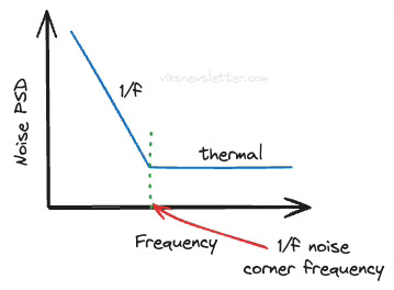
The frequency at which flicker noise reaches the same level as thermal noise is called the 1/f noise corner frequency. Ideally we want this corner frequency to be as low as possible, but modern MOS devices have high 1/f noise corners; even up to the 10-100 MHz range.
Gate Noise
The gate of a MOSFET is often a significant contributor to noise, and its effect is more important as the gate length is scaled down. Hence, good layout practices are required.
The polysilicon gate is not inherently a good conductor and has an appreciable amount of resistance associated with it. From a processing standpoint, most of the gate is specially processed by “siliciding” it to minimize its resistivity.
As we already know, any such parasitic resistance has a thermal noise associated with it. Due to the distributed nature of the gate along a transistor, we can think of the gate as having an effective resistance Rg,eff, whose associated thermal noise is
Approximately finding Rg,eff is simple. If you know the resistance-per-square of the polysilicon gate, estimate its DC resistance by counting the number of squares along the direction of the width of the transistor. Using 1/3rd of that DC resistance is a reasonable estimate for Rg,eff.
At either end of the gate, there is a metal contact that connects the gate to upper level metals. To further lower the gate resistance, the gate is contacted on both ends of the transistor. In this case, the Rg,eff drops to 1/12th.
Often, the resistance of this contact becomes the limiting factor in the noise of the transistor. Nothing can be done from a layout standpoint, other than maybe using multiple contacts to minimize the resistance even further.
When picking a transistor for low noise, designers almost always use the minimum device width they can get away with. In addition, multiple fingers are used in parallel to minimize the gate resistance especially for RF applications. One such multi-finger transistor layout is shown below.
Induced Gate Noise
This one is interesting. Remember that the space between the gate and channel of transistor is separated by a thin oxide layer. This makes the channel and the gate capacitively coupled, and if the frequency of operation is sufficiently high, there is a low impedance coupling path between the channel and the gate.
This means that any thermal noise in the channel induces a noise at the gate through the capacitive coupling path and its PSD can be expressed as:
where Cgg is the effective gate capacitance. Induced gate current noise has a squared relationship to the frequency. When using thin oxide, short channel transistors with high gate resistance and capacitance at high frequency, induced gate noise is a significant contributor to overall noise.
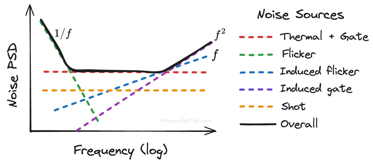
Similarly, the 1/f noise from the transistor will also be induced at the gate, with the frequency-squared dependence making it effectively proportional to frequency. Luckily, these mechanisms are at odds with each other. 1/f noise is low at high frequency, and the capacitive coupling is low at low frequency. As a result, induced flicker noise is not a major contributor.
Shot Noise
As the channel length of transistors shrink, there is an additional source of noise to worry about. The leaky gate oxide causes the carriers in the channel to tunnel through the oxide resulting in a gate leakage current. This quantum-mechanical effect will result in a shot noise contribution to the overall gate current noise and is related to the gate leakage current as:
Fortunately, the impact of shot noise is dominated by gate resistance noise and induced gate noise at RF frequencies of a few GHz. At frequencies below the GHz range, shot noise may become a significant source of noise. If you tied the source and drain of a MOS transistor together to make a capacitor, the shot noise of gate current will be a dominant noise source.
Now that there is gate leakage through the oxide dielectric, the resulting DC gate leakage current generates its own thermal noise and 1/f noise contributions to the gate current. The origins of 1/f noise in gate tunneling current is not well understood. It is best to let sleeping dogs lie for the sake of this article.
🔑 Key Takeaways
Channel and gate thermal noise are the most dominant sources of noise in a transistor operating at RF frequencies.
At low frequencies, flicker and shot noise are important. Due to up conversion in an RF system, they can become important at RF frequencies too.
Noise sources in the transistors are correlated to each other. The correlation is represented as a complex coefficient. We have not addressed that here.
Good transistor layout practices are important to minimize noise from parasitics.
📚References
RF Microelectronics by Behzad Razavi, Chapter 2.3.
Noise Sources in Bulk CMOS by Kent Lundberg.
A. J. Scholten et al., "Noise modeling for RF CMOS circuit simulation," in IEEE Transactions on Electron Devices, vol. 50, no. 3, pp. 618-632, March 2003.
M. J. Deen et al., "High-Frequency Noise of Modern MOSFETs: Compact Modeling and Measurement Issues," in IEEE Transactions on Electron Devices, vol. 53, no. 9, pp. 2062-2081, Sept. 2006.
Most textbooks use gm, the transistors transconductance to represent drain thermal noise. Using gd0, the output zero-bias conductance is a more accurate representation for a transistor in saturation. Read “Thermal Noise in Field-Effect Transistors” by A. van der Ziel, Proc, of IRE, 1962.
The views, thoughts, and opinions expressed in this newsletter are solely mine; they do not reflect the views or positions of my employer or any entities I am affiliated with. The content provided is for informational purposes only and does not constitute professional or investment advice.


Very interesting summary. What I missed is some line or two concerning the RTN/RTS type of noise (Random Telegraphic Noise). I have discussed lately with some people concerning the design of CMOS ASIC and when I brought up this concept of RTN, they never heard of it. Maybe this is something that is rarely a problem nowadays then???
So, reading between the lines, these modern tiny VLSI CMOS are not the nicest to use for audio or ancient radios like AM or FM? I remember discrete transistors where shot noise was a low rumble in audio range, but now you say the corner might be 100MHz, unreal.