A Brief History of RF Switch Technology
From PIN diodes, RF MEMS, MESFETs, and HEMTs to RF silicon-on-insulator technology, how the evolution of a circuit as simple as a switch is much more complex than it seems like on the surface.
A switch is supposed to be simple — on or off.
In the digital realm, we know how transistors are utilized to generate binary logic. However, an RF switch is a separate beast, with unique needs based on its position in the RF signal chain. These switches and the technology that powers them are so complicated that multimillion-dollar companies have emerged solely to design and manufacture them.
In this post, we'll take a brief trip down memory lane to discover how these switches evolved and gain an appreciation of the these deceptively complex devices.
Here is what we will cover:
RF switches and their key metrics
PIN diodes
Compound semiconductors
RF MEMS
RF Silicon-on-Insulator (SOI)
Read time: 11 mins
RF Switches and Their Key Metrics
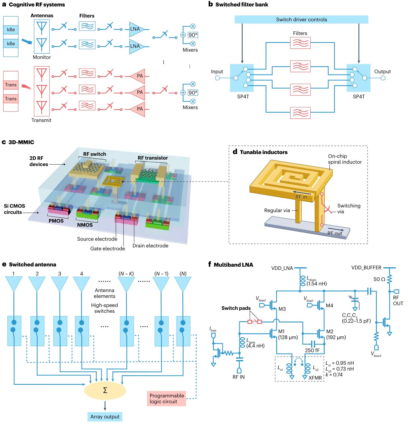
RF switches are largely responsible for managing the flow of signals in a radio system. With each succeeding generation of communication technology, we have added more geographically unique frequency bands. A new 5G smartphone must support more than 50 different frequencies while being portable. We discussed this in a prior piece.
What differentiates them from the ordinary on/off switches we're used to in digital logic? The answer lies in determining what signals these switches should allow or reject. RF switches must manage the flow of quickly varying radio signals, sometimes with high amplitude, while losing little to no power through dissipation.
Here's a list of RF switch-related terminology and what they mean:
Insertion Loss is the amount of power lost due to dissipation while the switch is turned on. It must be as low as possible because some received signals are already weak, with limited room for additional loss due to switching.
Isolation refers to the ability of a switch to prevent signal flow when it is turned off. It should be as high as possible so that no unwanted signal passes through the switch when it is supposed to be turned off.
Power handling of a switch refers to the highest amount of power that it can withstand. In the off state, it is the amount of power that the switch can sustain without turning on or breaking down. In the on state, it is the amount of power that the switch can withstand before high current through the device melts it owing to electromigration or other thermal effects.
Linearity refers to a switch's ability to faithfully transfer a signal from input to output when turned on, or to generate no stray signals when turned off. For example, with a single input, many output (single-pole multi-throw) switch, when one path is activated, the others are turned off. The on path should function as a linear, low-valued resistor, whereas the off switches should not be nonlinear elements.
Integration refers to the simplicity with which switches can be interfaced with other radio blocks and controlled. If the switch cannot be implemented as an integrated circuit, it must be packaged and put on an RF module, such as an interposer or a PCB. If it is CMOS-based, the integration level is significantly higher.
The frequency range of ideal switches should be frequency independent, spanning from DC to high frequencies. This is rarely the case, as we will discover. Some technologies have intrinsic low frequency limitations, whereas at higher frequencies, there is increased insertion loss and reduced isolation.
Switching time refers to how quickly a switch turns on or off when bias is altered. Depending on the transport or actuation mechanism employed, the time required for a switch to change states can range from tens of nanoseconds to a hundred microseconds. The consequences of switching time have an impact on the radio system that the switches are employed in.
The Ron-Coff product is a metric that measures how good any switching technology is. The product of on-resistance and off-capacitance, commonly measured in femtoseconds, should be as low as possible.

Silicon-on-Insulator (SOI) transistors made with CMOS technology are currently the most common solution for RF switches. RF-SOI technology is an obvious winner due to its integration with other silicon-based circuits and ability to scale to volume production at a reasonable cost. Exotic switching technologies have recently emerged, including gallium nitride, phase change materials, and 2D semiconductors. We will eventually go over all of them in depth at some point in this newsletter.
In this essay, we'll look back before we move forward.
PIN Diodes
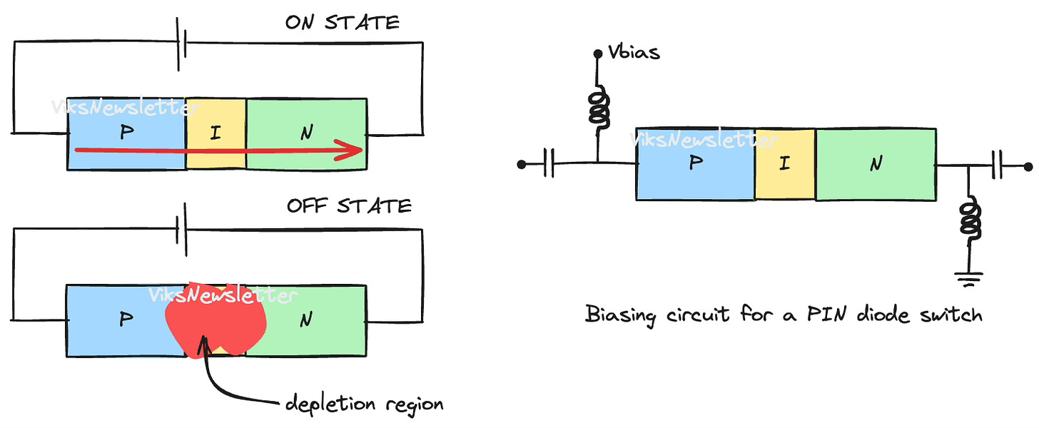
In the 1950s, a P-type, Intrinsic, N-type (PIN) diode was one of the first solid-state switches to replace bulky and cumbersome electromechanical switches. PIN diodes are made up of an intrinsic (undoped) silicon layer sandwiched by p and n doped silicon.
When forward biased, the intrinsic silicon fills up with electrons and holes, and current flows from p-type to n-type silicon. In the on-state, the diode has a forward resistance, which causes some energy to be dissipated. When reverse biased, semiconductor junctions get depleted of carriers, resulting in an electric field that opposes the flow of current.
A PIN diode has several major limitations as an RF switch.
Low frequency operation: The intrinsic region contains both electrons and holes, which begin to recombine if their variation is too slow. At low frequencies, a PIN diode in the on-state stops operating as a low-valued resistor and begins to function as a rectifier. In the OFF state, it operates as a nonlinear variable capacitor, reducing the switch's linearity.
High current consumption: The on-state resistance of a PIN diode is only low when a significant DC current flows through it. In other words, it is power-hungry.
Inconvenient biasing: Because DC and RF signals must travel through a two-terminal device, external biasing components are required to keep them separated. This increases the bill of materials, cost and footprint.
Compound Semiconductor Switches
MESFETs
For RF switching, Gallium Arsenide (GaAs)-based FET devices supplanted PIN diodes in the 1980s. Early switching devices were essentially MEtal Semiconductor FETs (MESFETs), which consisted of an n-type doped GaAs material on a GaAs substrate and metal gates. When the gate is biased above its threshold, a conducting channel forms, allowing signals to pass through with a low resistance between drain and source (RDS). When biased below the threshold voltage, the channel is pinched off, which implies that it is depleted of carriers and no signal flows.
pHEMTs
The on-state resistance of MESFETs were not great. Thus, pseudomorphic High Electron Mobility Transistors (pHEMTs) were born. These devices are essentially FETs but contain a semiconductor heterojunction, which uniquely lowered the on-state resistance of the switch.
The cause for drop in resistance is the formation of a very thin layer with extremely high electron mobility1 when two materials with different bandgap energies are layered (for example: AlGaAs and GaAs). The interface is a 2-dimensional electron gas which provides a generous amount of readily available electrons for conduction. As a result, pHEMT switches demonstrated outstanding low-loss performance in the on-state.
One disadvantage of early pHEMT switches was gate lag. When voltage was applied to actuate the switch, it would do nothing for several hundred microseconds, and then suddenly flip states. This happened because of traps in the heterojunction interface that would randomly capture electrons and not let them conduct. When the persistent field cannot hold back electrons any more, it would suddenly turn on. Today, proprietary techniques have almost eliminated gate lag issues by properly engineering the transistor structure (a secret recipe for many pHEMT manufacturers).
GaN
Today's cutting-edge HEMT switches use gallium nitride (GaN) as a semiconductor material. This material's wide bandgap allows it to withstand extremely high voltages without breaking down, while also giving good RonCoff performance for high frequency applications. Inherently, GaN has lower electron mobility than GaAs pHEMT. However, the power handling characteristics of GaN make it an appealing option today.
Micro-ElectroMechanical Switches (MEMS)
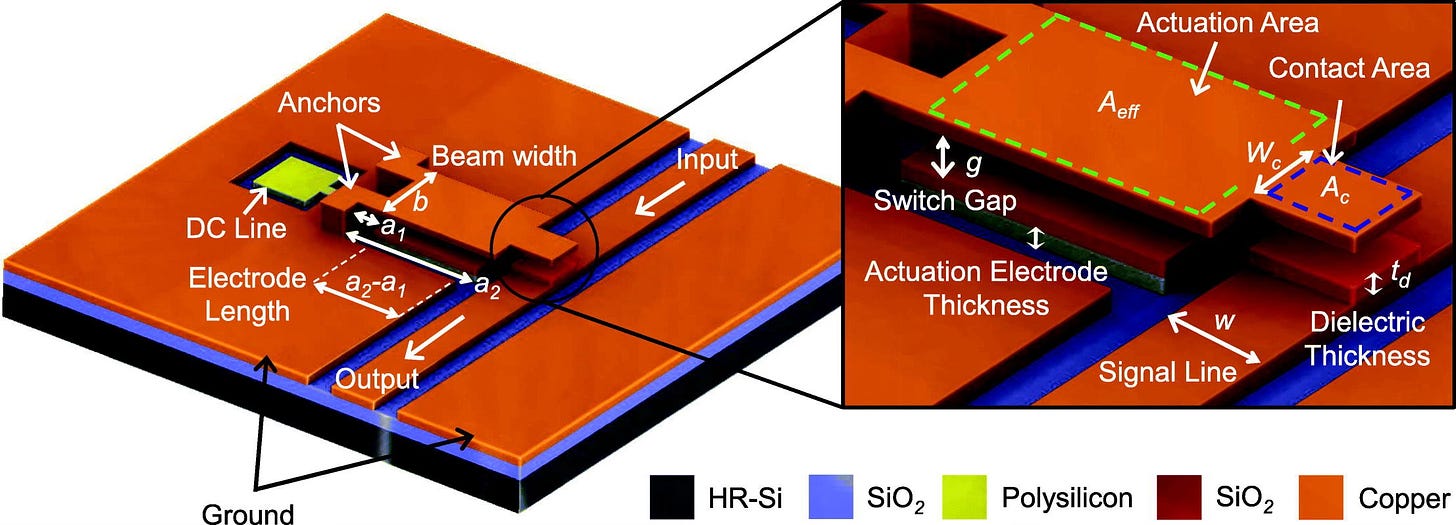
In the early 2000s, RF MEMS emerged as an alternative to PIN diodes and HEMT switches. RF MEMS is the fabrication of microscopic metal plates hanging above an electrode that can be moved by providing a voltage between the electrodes. Contacting the two electrodes turns on the switch. Because MEMS switches lack semiconductors, they can achieve Ron-Coff values that are orders of magnitude lower than transistor-based switches, making them ideal for high-frequency applications.

They do have a few disadvantages.
Actuation voltage: Early RF MEMS switches required almost 50 volts to operate. Because the actuation was electrostatic, there was no current draw and no power consumption issues. However, generating such high voltages in applications was not an attractive prospect. With proper engineering of mechanical structures, these voltages have been reduced to just under 10 volts today. This is still too high considering transistor based switches actuate at 3 to 5 volts.
Switching time: Because the actuation is mechanical, switching time is microseconds rather than nanoseconds in semiconductor switches. This is the fundamental constraint of mechanical switches. It is not easy to improve switching times by an order of magnitude.
Reliability: Early on, reliability was a concern with the moving parts related to RF MEMS switches. With considerable effort on reliability engineering, today's RF MEMS switches survive over a billion actuations. This is a problem that has more or less been solved in RF MEMS.
Packaging and Integration: RF MEMS switches were originally fabricated on glass substrates and required hermetic (airtight) encapsulation. They were also highly susceptible to electrostatic discharge (ESD) damage since ESD protection diodes could not be included with complex packaging requirements. Today, firms such as Nanusens have developed RF MEMS switches on a conventional CMOS line, allowing for some truly fascinating devices in the next generation of communication devices.
Silicon-on-insulator (SOI) Switches
If you're wondering, why not just use ordinary CMOS transistors as switches? Don't we have cheap costs, high yields, and integration with other silicon circuits? That is because the semiconducting silicon substrate is unsuitable for RF. The transistor breaks down at low voltages, the poor semiconducting substrate prevents stacking switches in series to properly distribute the voltage, and there are eddy current losses in the substrate. No one really makes RF switches using sub-10nm-class nodes that make all the news these days.
Sapphire
The solution to the problem of poor substrate is to simply use a better one. Thus, silicon-on-insulator was born. While it had its early origins in US naval research labs, Peregrine Semiconductor2, was among the first to commercially build RF switches on sapphire substrates. Sapphire is a perfect insulator, and was ideal for RF applications. But it was expensive as a starting material.
High Resistivity and Trap Rich Silicon
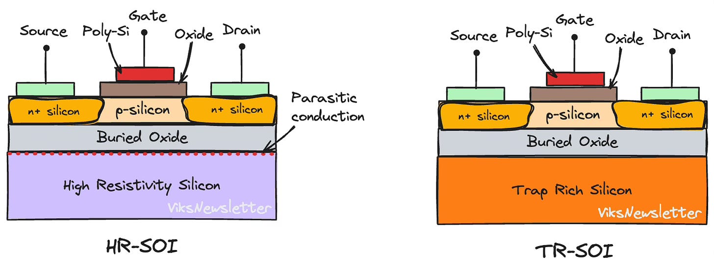
This paved the path for the use of classic silicon substrates that had been modified to increase resistivity (more insulating substrates) above standard bulk silicon. When RF switches were first developed on high resistivity silicon, they did not work very well. A substrate with 1000 ohm-cm resistivity behaved as if it were 100 ohm-cm, or thereabouts.
It was eventually determined that the interface between oxide and high resistivity silicon caused parasitic conduction effects, lowering the resistivity. High resistivity silicon wafers need more treatment to prevent parasitic conduction effects, resulting in trap-rich SOI substrates.
The main idea was to introduce traps by passivating the interface, leaving positively charged dangling covalent bonds that caught free electrons and prevented parasitic conduction. In the current market, SOITEC has monopolized the supply of these trap-rich wafers, which they call Smart-Cut technology. The specific methods for passivating the interface are trade secrets.
Today, RF-SOI is the preferred technology for switches in integrated RF front end circuits, and it is found in practically all mobile devices available today. Transistor sizes most often range from 22nm to 180nm depending on the application, as each transistor must withstand a 3 to 4 volts of voltage swing across it. They can then be stacked in series to create switches capable of tolerating larger voltages. However, stacking increases the overall resistance and insertion loss of the switch. The design of these switches involves a complex trade-off.
If you believe I missed any aspects of RF switch history, or have any factual errors, please respond to this email and let me know.
If you like this post, please click ❤️ on Substack, subscribe to the publication, and tell someone if you like it. 🙏🏽
If you enjoyed this issue, reply to the email and let me know your thoughts, or leave a comment on this post.
We have a community of RF professionals, enthusiasts and students in our Discord server where we chat all things RF. Join us!
The views, thoughts, and opinions expressed in this newsletter are solely mine; they do not reflect the views or positions of my employer or any entities I am affiliated with. The content provided is for informational purposes only and does not constitute professional or investment advice.
Mobility is a metric of how fast an electron moves in a metal or semiconductor when an electric field is applied.
Now pSemi after the Murata acquisition. I worked here from 2011-2016.


