Ruthenium: The Next Step in Interconnects for Advanced Logic Nodes?
Why ruthenium is emerging as an alternative to copper for low-level metal interconnects as pitch drops below 20-nm in sub 2-nm class advanced technology nodes. Also, haven't we heard this song before?
As transistor nodes scale below 2nm, copper interconnects have become a limiting factor in both size and electrical performance, and future leading edge nodes are likely to use ruthenium (Ru) instead of copper (Cu).
Last month, at the International Electron Devices Meeting (IEDM) 2024 held in San Francisco, Intel unveiled a “subtractive” ruthenium process with special methods to reduce line-to-line capacitance between metals smaller than 25 nm in pitch. To quote their press release (emphasis mine),
To help improve the performance and interconnections within chips, Intel Foundry showcased subtractive ruthenium, a new key alternative metallization material that uses thin film resistivity along with airgaps to deliver a significant advancement in interconnect scaling. The team was first to demonstrate, in R&D test vehicles, a practical, cost-efficient and high-volume manufacturing compatible subtractive Ru integrated process with airgaps that does not require expensive lithographic airgap exclusion zones around vias, or self-aligned via flows that require selective etches. The implementation of airgaps with subtractive Ru provided up to 25% of line-to-line capacitance reduction at pitches less than or equal to 25 nanometers (nm), illustrating the benefits of subtractive Ru as a metallization scheme to replace copper damascene in tight pitch layers. This solution could be seen on Intel Foundry’s future nodes.
In this article, we will understand the advantages of ruthenium over copper as interconnect dimensions shrink, and look back at how it worked out last time for Intel.
For free subscribers:
The problem with copper interconnects
Subtractive vs dual-damascene etch
RC-parasitic limitations in copper interconnects
Material advantages of using ruthenium over copper
Bulk resistivity
Mean free path
Cohesive energy
For paid subscribers:
Subtractive ruthenium lithography
Fully Self-Aligned Via (FSAV/FAV) Semi-Damascene (IMEC)
Top-Via (IBM)
A strange cobalt deja-vu (how it didn’t work out for Intel)
Conclusions
References/Further reading (12 articles, 5 papers)
Read time: 13 mins
Quick note: You can read the full version of this article by upgrading to a paid subscription for $99 for one year (34% discount) . This limited-time promotional pricing is available for another week (till Jan 14th), and is my way of thanking early supporters of this newsletter. Your support means the world to me.
The Problem with Copper Interconnects
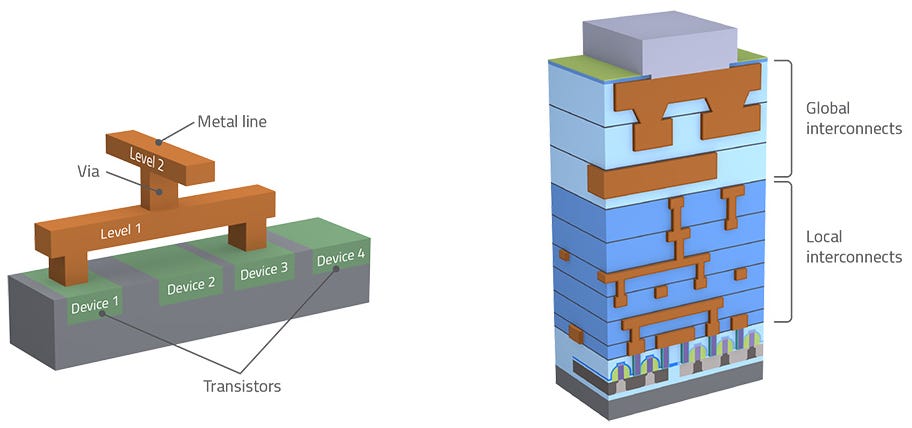
Copper has been the material of choice for the last three decades for creating tiny metal wires called interconnects to wire up the transistors properly, interface them with other circuits and the outside world. Interconnects on a chip are multilayered, with advanced transistor nodes having 12-15 metal levels patterned on the wafer to enable complex multi-level connections within the chip. Also, rising transistor density following Moore’s law dictates that transistors in any technology node be placed as closely as possible to pack as many transistors as possible on a chip. As transistors get closer together, the metal lines connecting to them also get smaller in feature size. This is especially a problem in lower level metal interconnects. Higher up in the chip however, it is not of much concern.

Subtractive vs Dual-Damascene Etch
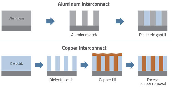
When copper replaced aluminum in the late 1990s, its superior electrical conductivity offered significant improvements in resistance of the interconnects. In addition, they could be patterned to provide smaller feature sizes to keep pace with shrinking transistor sizes. Interestingly at the time, the way copper was patterned was different from how aluminum interconnects were created.
With aluminum interconnects, the aluminum is first etched away to create wire interconnects and then the gap filled in with dielectric material for insulation. This is called a “subtractive etching” process.
When using copper, a “dual-damascene” process was required to pattern interconnects (damascening is the process of inlaying one metal into another). First the dielectric had to be deposited, then selectively etched away to create trenches where metal interconnects will exist. It was then filled with copper using electroplating and finally polished to remove excess material. This is the simplistic explanation of the process; we will delve into a bit more detail later. Clearly, this was more complex than patterning aluminum, but the performance gains were worth it.

RC-Parasitic Limitations in Copper Interconnects
As transistor gate lengths scaled to smaller values, starting somewhere around the 14 nm node and getting really worse at 5 nm and below, interconnect performance started to become a bottleneck for two reasons:
Resistance: the copper lines that had to be patterned were getting too small, and a smaller cross-sectional area for current to flow meant increased resistance, greater voltage drop and higher thermal dissipation.
Capacitance: when copper lines got too close together, their cross talk started to increase, resulting in a slowing down of the chip’s core performance due to interconnect bottlenecks. To reduce capacitance, “low-k” dielectric materials with reduced relative permittivity (εr) were introduced. The materials had εr values of about 2.5 compared to 4.2 for silicon dioxide dielectric and hence provided some improvement in crosstalk levels.
But there was no way to solve the resistance problem. In fact, it got significantly worse due to the way copper was actually deposited in a dual-damascene process.
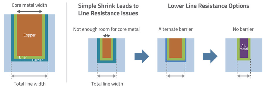
The actual process of creating copper lines is much more than simply putting copper in dielectric trenches. First, a barrier layer (dark blue), typically tantalum nitride, needs to be deposited in the trench to prevent the copper metal from diffusing into the dielectric. A tantalum or more recently a cobalt liner (light green) is then deposited to improve the adherence of the barrier to the metal. Next, a copper seed layer is deposited to initiate the electroplating process. Finally, bulk copper is electroplated to fill the trench.

When these additional materials are used, the overall resistance of the copper line drops for two reasons:
The barrier and liner materials are not good conductors of electricity, and they increase the effective resistance of the copper line.
The cross-section of low-resistance copper is reduced by about 2nm on each side, or 4nm in all, which itself leads to increased resistance. This poses a problem when the adhesion layers make up about 30% of the interconnect line width, which can be around 10 nm with a pitch under 25 nm. As the table shows below, future technology nodes are projected to have even smaller metal pitches approaching 10 nm.
It is not trivial to make the barrier and liner thinner because any accidental gaps or voids in the barrier results in reliability issues. There is considerable ongoing research on improving the performance of copper lines in sub 5-nm class process technologies which we won’t get into here. Using a material that does not require a barrier layer is an effective way to increase interconnect cross-section and lower resistance. Ruthenium is emerging as a promising candidate, and there are reasons why.
Material Advantages of using Ruthenium
The problem of choosing the right interconnect metal is as much a material science problem, as it is an electrical one. We will compare ruthenium to copper under several different lenses.
Bulk resistivity
This is a fundamental material property expressed in units of μΩ-cm that depends on the atomic structure of the metal and the mobility of the electron within its crystal structure. Ideally, we want bulk resistivity to be as low as possible for an interconnect metal. Copper has an excellent bulk resistivity of 1.68 μΩ-cm, which is why it has been the primary choice for CMOS interconnects. Ruthenium has a much higher bulk resistivity of 7.1 μΩ-cm and is a poorer choice of metal compared to copper, but is still a leading candidate for the future of interconnects because of how its resistance behaves at nanoscale dimensions as we will see next.
Mean free path
Mean free path (MFP) is the average distance travelled by an electron in a material before it encounters scattering events due to collisions with atoms, surfaces or grain boundaries. For nanoscale interconnects, we want MFP to be as low as possible. This means that the resistive properties of the metal is insensitive to shrinking dimensions. For metals with high MFP, scattering at surfaces and grain boundaries increases as size shrinks and resistivity dramatically increases.
Copper has a relatively high MFP of ~40 nm which implies that its resistance severely increases due to frequent scattering when interconnect dimensions are scaled to ~10 nm. In contrast, ruthenium has a low MFP of ~6-8 nm which makes it less sensitive to resistance increase at small dimensions and more suitable for narrow interconnects at advanced technology nodes. So while ruthenium has a higher bulk resistivity, its low MFP makes it a better choice for very small feature size interconnects.
Cohesive energy
Cohesive energy is a measure of how strong the bonds between atoms are in a material, and is usually measured in electron-volt per atom (eV/atom). Higher cohesive energy is preferred because it means that the atoms are less prone to movement under external stresses induced by current flow. Ruthenium has a high cohesive energy of ~6.7 eV/atom, while copper’s cohesive energy is only moderate at ~3.5 eV/atom. The higher cohesive energy provides two major advantages for ruthenium over copper:
Lower diffusion: Since ruthenium atoms are strongly held together, they are less prone to diffuse into the surrounding oxide when deposited into dielectric trenches during damascene processing. As a result, ruthenium can be used without barrier layers which buys back much of the cross-sectional area for current flow that was lost when using copper. This is a significant advantage at small interconnect dimensions because the resistance increase brought about by higher bulk resistivity of ruthenium is recovered from its increased conduction area.
Better electromigration resistance: Electromigration is the movement of atoms brought about by current flow in an interconnect and often presents reliability concerns due to formation of opens and shorts in small interconnects. The higher cohesive energy of ruthenium implies that the atoms are less prone to movement compared to copper, and thus provide better resistance to electromigration effects.
Subtractive Ruthenium Lithography
A major advantage of ruthenium is that it can be patterned with subtractive etching much like in the early days of aluminum interconnects.


