ABCs of Power Amplifier Classes: Foundations
Basic concepts required to understand classes of operation in power amplifiers.
Hey, I’m Vikram 👋!
I have realized that it is much better for the content of this newsletter if I can hold a train of thought on a particular topic. Electrical engineering is complex to explain, and the articles will benefit from having sufficient depth by not rushing through the explanations. As a result, future posts will often be part of a collection of similarly themed articles.
Some housekeeping:
We recently crossed 3000 subscribers in this publication. Thank you for your readership.
I will be taking a 2 week summer break from writing this newsletter to prevent burnout.
Please join our Discord server where we already have an RF community with 30+ people.
If you like this post, please click ❤️ on Substack. The algorithm will then show it to more people. This is an easy way to support this publication.
In this series, I'd like to discuss power amplifiers, and since the scope can be very large, we will focus on amplifier classes labeled by alphabet. Not all letters in between are amplifier classes, not all are even RF (they're audio range), and we might even argue about whether thats how a particular class is defined. But herein lies the fun.
This series is an ambitious undertaking and will take many articles to cover to the level of depth I envision. It might happen that each of these articles takes longer than one week to write, and are published across different time intervals, not necessarily in linear fashion. Please consider subscribing to the newsletter to have all posts delivered to you.
It is not easy to define a specific power level after which an amplifier becomes a "power amplifier (PA)." For example, a cell phone amplifier outputs about 1 watt, audio amplifiers output hundreds of watts, while low power bluetooth circuits might output only 10 milliwatts. An amplifier at any output power can be made to operate in different classes, depending on the needs of the application and the performance we desire from it.
Before we dive into the deep end, we need to set the stage with the proper concepts that we will constantly mention in this series. These ideas are the foundations on which we will build upon. As simple as some of these topics might seem, it is still worth dedicating a post to.
This article is part of a series on power amplifier classes of operation. You can jump to any article using the links below:
Foundations (this article)
Specifically, we will cover:
IV-relationship of an active device
Load lines (DC / AC / static / dynamic)
Conduction angle
Efficiency
Read Time: 9 mins
Current-Voltage (IV) Relation of an Active Device
First, we need to understand the ideal operating behavior of an active, amplifying device. This is the foundation on which amplifier classes and operation will be defined.
In general, an active transistor generates current when a voltage is applied to it. For a bipolar transistor with a voltage at its collector, injecting a base current results in a large collector current. The ratio of collector current to base current is called the current gain, β. Bipolar junction transistors can be made on silicon, or they can employ heterojunctions such as Silicon-Germanium (SiGe) or Gallium Arsenide (GaAs).
For a field-effect transistor (FET) with a voltage at the drain, increasing the gate voltage above a threshold value causes drain current to flow. The amount of drain current for a change in gate voltage is called transconductance (often represented as gm). The FET can be made on silicon, such as a bulk-silicon or silicon-on-insulator (SOI), or it can be made on GaAs using pseudomorphic high-electron mobility transistors (pHEMTs). A more recent development involves the use of Gallium Nitride (GaN) FETs, which provide high power operation.
The current-voltage relationship of an ideal MOSFET looks like in the figure below. A similar characteristic can be drawn for bipolar transistors.
Real devices do not behave in such an ideal fashion, but we will describe transistor operation in a simple way, so we can keep our eye on the prize - amplifier classes.
Vk is the knee voltage, after which increasing drain voltage will not increase the current because it is in saturation. Below knee voltage, the device is basically a gate-voltage controlled resistor.
Vt is the threshold voltage on the gate, which is the minimum value of voltage needed to make the device conduct. Below this value, the device will be in the cut-off region, and there will be no current. For a given drain voltage, increasing gate voltage beyond saturation voltage (Vsat) will not increase drain current.
Imax is the maximum value of current that the device is capable of supplying.
When the device is above cut-off but hasn't its maximum drain current Imax yet, the device is said to operating in the quasi-linear region.
Ideally, we want a device that can provide a high value of Imax, have a low knee voltage, and equally spaced, flat lines on the Id-Vd space as the gate voltage is increased. In the Id-Vg space, we want a linear relationship between current and gate voltage in the quasi-linear region.
Load Line
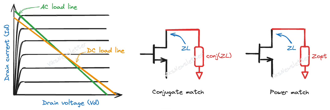
An amplifying device converts the output current into a voltage only when a load is placed at its output. The choice of this load affects the voltage-gain and total power extracted from the output of the transistor. On the IV space, the load-line is a diagonal line whose slope depends on the load value.
In reality, the load is a complex value and is constructed as a combination of inductors, capacitors, transformers and resistors. As a result, the AC load line is usually different from the DC load line because the presence of reactive elements results in a different load line that varies with frequency compared to a purely resistive DC load.
The load network is a usually a carefully designed, complex impedance. There are two fundamental methods to design load networks (although it can get very complicated in actual amplifier designs):
Conjugate Match: The load impedance is designed to be the complex conjugate of the device output impedance.
This provides maximum power transfer from the device to the load provided that the active device has no limitations on the power it can deliver.
This is usually not an issue for low-power amplifiers because the devices are not pushed to deliver high power. They can always deliver the instantaneous current and voltage expected of them. As a result, a conjugate match is usually the right choice for the load.
Power Match: The load impedance is designed to deliver maximum power to the load, while considering the power limitations of the device.
This is usually not the complex conjugate of the device impedance. Even if the complex conjugate ensures maximum power transfer from the device, it will not be possible if the device is required to deliver more instantaneous voltage and current than it is capable of. Due to power limitations imposed by the device, the power delivered will drop.
Instead, there is another optimal impedance called the power match that will ensure maximum power at the output while taking power limitations of the device into account. This is often experimentally determined with a special measurement called load-pull.
As an aside, in an earlier article, we looked in-depth into how various input and output match conditions define the gain from an amplifying circuit. Give it a read.
Static and Dynamic Bias Point
A classical amplifier that uses an amplifying device with a load at its output, is biased at a specific voltage and current setting called its quiescent bias point, that lies on the load-line. This is a very important choice for amplifier operation, and we will see why when we define various amplifier classes later in this series.
If the amplitude of the input RF signal is low enough and gain isn't too terribly high, the devices might not be sufficiently disturbed from their quiescent bias condition. It can be considered to be static during amplifier operation. This is usually the case in low power amplifiers, such as low-noise amplifiers.
For medium and high-power amplifiers, the bias point will move with the input RF signal, or if the output signal swing is high enough, with the output RF signal. In such a scenario, we need to think of a dynamic IV space where the bias point will instantaneously reside during the process of amplifying an RF signal. This complicates matters because:
the amplifier operation starts being non-linear
the IV behavior itself might change based on the previous bias point it was in (this is called memory effect).
We won't get into all the complexities right away, but it is useful to form a clear mental picture of what goes on at a device level.
Conduction Angle
A common approach to classifying amplifier operation is based on conduction angle.
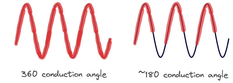
Conduction angle is the total phase angle of a sinusoidal signal for which the transistor is kept in operation, or equivalently, in conduction, where it consumes DC power.
If the transistor is always conducting for all phases of the input sinusoidal signal, the conduction angle is 360 degrees. If the transistor is placed in cutoff for part of the signal cycle, then the conduction angle will be less than 360 degrees.
Depending on how long the transistor is kept conducting, we will later classify amplifier operation into class A, B, C, and so on. The main idea behind turning off transistors for part of the time is to save on DC power dissipation, and improve efficiency of the amplifier (we’ll discuss this next). While efficiency improves when transistors are partially turned off, the output signal is more distorted. There is a constant trade-off between linearity and efficiency.
Efficiency
Efficiency is a metric of great importance for a power amplifier, and is loosely a measure of how much of the supplied DC power is converted to RF power at the output. An efficient amplifier converts most the supplied power into RF, and implies better battery life for handheld devices, and lower heat generation in the active devices.
There are two important efficiency metrics we need to define:
Power Added Efficiency (PAE): It is the ratio of the output RF power after accounting for the gain of the amplifier, to the DC power supplied to the amplifier. This is a more general definition that is applicable to all amplifiers regardless of their gain level.
Drain Efficiency (DE): It is the ratio of the output RF power to the DC power supplied to the amplifier. This definition is valid only when the gain is sufficiently high such that the output power is much higher than the input power. For example, drain efficiency approaches PAE when the gain is 1000x (or 30 dB), in which case, ignoring the input power is a negligible source of error.
Many engineers and even vendors erroneously use these efficiency definitions interchangeably regardless of amplifier gain. So always make sure to clarify with your colleagues or vendors what efficiency definition being referred to.
While this article might seem like a collection of partially connected concepts, they will come together when we discuss class A amplifiers in the next article.
See you then.


Hi Vikram,
Thank you very much for your blog; it is truly educational. Could you please share your expertise on the two-tone test and the calibration methods used to maintain the linearity of power amplifiers within the dynamic range? Additionally, I would appreciate your insights on how third-order intermodulation distortion (IMD3) is interpreted in relation to nonlinearity. Also, any thoughts on methods to determine bias voltages that can be adjusted as a function of temperature?
Respectfully,